Scientific EMCCD cameras have demonstrated excellent imaging performance under extreme low light conditions. Photon counting capability combined with a very low dark current offered by the CCD technology have made EMCCDs the detector of choice for high-performance applications such as time resolved spectroscopy and low light imaging. However, future astronomical instrumentation requires high spatial resolution while commercially available EMCCD devices are limited by a relatively modest area format of (1k×1k). To address this requirement, the Universite de Montréal and Teledyne-e2v have jointly developed a 4k ×4k EMCCD, the CCD282. This paper presents the results of cryogenic characterization of the CCD282 operated with Nüvü Camēras’ CCD Controller for Counting Photons version 3. The advantages of a novel large format EMCCD over existing technology for high resolution spectroscopy are discussed.
Since the introduction of the first commercial Low Light Level CCD by Marconi in early 2000,1 and shortly after the Impactron2 commercialized by Texas Instruments, several devices exhibiting an Electron Multiplication register to generate sub-electron read-out noise were developed. These Electron Multiplying CCDs (EMCCDs), from the CCD65 which was built in two variants for the PAL and NTSC video standards, to the CCD201-20 (introduced by e2v Technologies) and TC285 (introduced by Texas Instruments) of 1k × 1k image area, were falling short of pixels for scientific applications in extreme faint flux conditions requiring large field of view and high pixel count. For instance, very high resolution spectroscopy (R > 30000) can not be efficiently accomplished on a 1k×1k device. On the other hand, although wide field surveys could be accomplished with several small devices, the form factor of the existing EMCCDs (non-buttable) renders the use of the focal plane inefficient and reduces the advantages of using an EMCCD.
For those reasons, the Universite de Montréal, through a funding by the Canadian Foundation for Innovation (CFI), awarded a contract to e2v Technologies (now Teledyne-e2v) to develop a large format EMCCD. The end result, the CCD282, is a 4k × 4k device capable of generating ∼5 images per second with sub-electron read-out noise. This work presents the experimental setup developed at Nüvü Camēras to test this novel device as well as the preliminary characterization results.
The CCD282 is a standard silicon split-frame transfer EMCCD with an active region of 4096×4096 square pixels of 12µm3 (49.15 mm side length). The split-frame transfer architecture requires twice the area of the active pixels, since half of the pixels are masked by the store shield. Hence, the CCD282 is a large device, with a die size of 104×51 mm, and with a package size of 125×70 mm, which compares to the size of today’s smartphones.
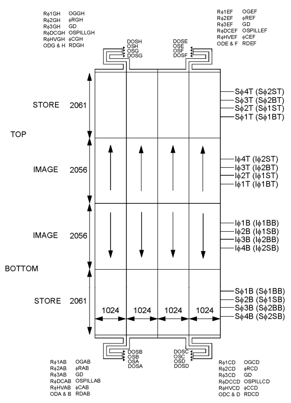
The image and store sections are designed to operate in 2-phase mode, each phase being clocked in pair (Figure 1). It provides 8 Electron Multiplying outputs that are specified to operate at up to 15MHz, which should yield 4–5 full frames per second at this frequency. Its large size limits the vertical line transfer rate to 166 kHz (6 µs per line). This yields a frame transfer time of ∼12 ms.
By comparison with well know EMCCDs such as the CCD201-20, the 1k × 1k device of Teledyne-e2v, the CCD282 has a few notable design differences. First, the CCD282 does not provide non-electron multiplication (conventional) output. Conventional read-out of the device is be possible by using a high voltage clock amplitude that is low enough to prevent Electron Multiplication. In this mode, no Excess Noise Factor will be generated. It must be noted that the device provides one dummy output for every output for optional differential use. The differential use does however increase the read-out noise by a factor of √2 as the noise of both outputs adds-up quadratically.
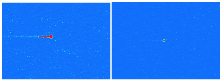
Next, the Dump Gate, which allow for dumping unwanted lines of signal, is not present. Although it is a useful feature to properly get rid of the dark current that has accumulated in the storage area during the integration period (which pile up in the horizontal register during the initial Frame Transfer), it does increase the capacitance of the horizontal register, which in turn renders the high speed operation of the device more challenging. On the other hand, an Overspill Drain has been included, which prevent an excessive level of charge from being generated in the Electron Multiplying register. This helps limit (or eliminate) the ageing of the multiplication register. Moreover, it does prevent, at high EM gain, the energetic cosmic rays from generating an excessive number of electrons, which eventually saturates the multiplication register and requires several clock cycles (and therefore, pixels) to be cleared (Figure 2).
Two PT1000 platinum resistance thermometers are glued to the device’s package, which provide a good temperature read-out of the Electron Multiplying registers, where the highly temperature-dependent electron multiplication process occurs.
Another noteworthy difference between the CCD282 and existing Teledyne-e2v’s EMCCDs is that it has been designed specifically for low flux applications. As a result, the pixel’s Full Well (FW) was measured to ∼20ke (see Section 4). The rationale behind this choice is that less electrons requires lower clock swing to shift them, and lower clock swings generates less Clock Induced Charges (CIC), which is the dominant source of noise in EMCCDs operated at a high frame rate. The large size of the device implies that the RC time constant of the polysilicon electrodes is quite high, which in turn prevent from using fast vertical clocks. As it has been shown that in Inverted Mode Operation (IMO) the generation of CIC is inversely proportional to the clocking frequency,4, 5 a conventional vertical clocking as slow as 166 kHz in IMO could have generated an unacceptable amount of spurious charges. Hence, the CCD282 was designed with Non-Inverted Mode Operation (NIMO) in mind, whilst not preventing its use in IMO. However, the NIMO operation involves the generation of a higher dark signal since the surface component is not suppressed. In the pursuit of the highest signal-to-noise (SNR), it is the total number of spurious charges generated (the total background signal) that matters, wether they arise from dark current or CIC. In this paper, we will present the total background signal measured on the CCD282 in both IMO and NIMO modes.
Although the CCD282 is made to be operated as a split frame transfer device, it is possible to read it out through a single side by clocking, say, Iϕ1T and Iϕ4T in phase, and Iϕ2T and Iϕ3T in phase, which will shift the electrons towards the bottom half image area rather than the top half store area. In this case, however, it would not be possible to use the bottom store area to hold the entire 4k × 4k image, so the bottom image area would hold the content of the top image area during the read-out. As a result, unless a shutter would be used, one would expect to have a superposition of the signal in the last half of the image being read-out.
3.1 Electronics
Referring to Figure 1, the CCD282 requires the supplying of the following signals to read it out:
• 16 vertical clocks (Sϕ1–4B, Sϕ1–4T, Iϕ1–4B, Iϕ1–4T);
• 12 low-voltage horizontal clocks (Rϕ1–3AB, Rϕ1–3CD, Rϕ1–3EF, Rϕ1–3GH);
• 4 high-voltage horizontal clocks (RϕHVAB, RϕHVCD, RϕHVEF, RϕHVGH);
• 4 reset clocks (ϕRAB, ϕRCD, ϕREF, ϕRGH);
• 4 clamp signals (ϕCAB, ϕCCD, ϕCEF, ϕCGH).
Moreover, the following DC voltages must be supplied:
• 4 Output Gate voltages (OGAB, OGCD, OGEF, OGGH);
• 8 Output Drain voltages (ODA, ODB, ODC, ODD, ODE, ODF, ODG, ODH);
• 2 Guard Drain voltages (GDB, GDT);
• 4 Overspill Drain voltage (OSPILLAB, OSPILLCD, OSPILLEF, OSPILLGH);
• 4 Reset Drain voltages (RDAB, RDCD, RDEF, RDGH);
• 4 multiplication register DC bias voltages (RϕDCAB, RϕDCCD, RϕDCEF, RϕDCGH);
• a Substrate voltage.
Finally, every eighth of the image data of the CCD282 will come out on the Output Signal pins (OSA-H) with the provision for using the eight Dummy Outputs (DOSA-H) to allow for the suppression of DC biases induced by the read-out process.
The electron multiplying registers are arranged in such a way that each horizontal clock, being low voltage or high voltage, is responsible for moving the electrons of two adjacent sections of the device. Hence, the amplitude of one high voltage clock will control the electron multiplication gain of two outputs.
The stock version of Nüvü Camēras’ CCCPv3 EMCCD controller has been designed to clock a CCD or EMCCD with up to four outputs. It has the capability to digitize 4 simultaneous video signals (120 MSPS, 16 bits each) and generate 14 low voltage analog clocks (14 bits, 4.16 ns refresh period), 2 high voltage clocks (25–50 V amplitude adjustable over 14 bits, 78 ps resolution), and 11 DC voltages (14 bits). Those resources are enough to drive a half of the CCD282.
Since it was expected that a large format EMCCD would eventually become available, the CCCPv3 has been designed with a spare connector populated with differential pairs to allow for several controller to be synchronized together. Thus, in order to clock both halves of the CCD282, the CCCPv3 firmware has been modified to make it stackable using a master/slave architecture. The modified design can support up to 8 synchronized controllers, with 7 slaves that are precisely phase aligned to the master. Communication to the synchronized controllers is done through a single serial data link to the master controller. The master controller has it’s own interface to all of the slaves. This allows the user to consider the controllers as a single entity with multiplied resources.
Stable and repeatable phase alignment of the controllers is critical for image consistency. It is achieved by locking the primary clocks of the slaves to the primary clock of the master. The resulting clocks are then aligned within a window of 78 picoseconds through all of the controllers. The design allows for the controller to be relatively far away from each other, since propagation delay of several clock cycles (4.16 ns native clock period) are supported between each controller.
This design feature has its advantages for clocking at a high speed (≥10 MHz in this case) a device as large as the CCD282, since the controllers can be located on each side of the device. This limits the propagation delay of the signals between the controllers and the side of the EMCCD they are responsible of clocking and prevents unwanted transmission line effects from affecting the signal integrity.
By synchronizing two CCCPv3 controllers, their combined ressources are sufficient to clock and read-out the entire CCD282 with the following trade-offs:
• The low voltage horizontal clocks are driven in pairs (on the bottom side, Rϕ1–3AB and Rϕ1– 3CD are driven commonly, on the top side Rϕ1–3EF, Rϕ1–3GH are driven commonly). This choice limits the horizontal clocking frequency of the CCD282 to 10 MHz since a higher frequency would exceed the output current capability of CCCPv3 clock drivers (each horizontal clock pin has a capacitance of ∼135 pF, which means that each clock driver sees ∼270 pF);
•The clamp signals are driven in pairs (on the bottom side, ϕCAB and ϕCCD are driven commonly, on the top side ϕCEF and ϕCGH are driven commonly);
• Since their nominal voltages are similar, the Guard Drains and the Overspill Drains are biased commonly for each half of the device (OSPILLAB, OSPILLCD, GDB are tied together, OSPILLEF, OSPILLGH and GDT are tied together).
This way, every controller is responsible of the clocking of a half of the CCD282 and, notwithstanding a ground plane on the CCD board that is shared between both controllers, there are no signal that have to be carried from one half of the CCD to the opposite controller.
3.2 Mechanics and cooling
When the CCD282 is clocked at its maximum frame rate, by using 166 kHz vertical clocks and 15 MHz horizontal clocks, it dissipates ∼3.4 W, from which about 800 mW comes from the real and dummy output circuits. In order to cool the CCD for the experiments, it was not convenient to use a Thermoelectric Cooler, and a mechanical housing consisting of a Liquid Nitrogen (LN2) cryostat with a customized head was built. The entrance window of the cryogenic head is compatible with the M95 lens mount. The two controllers are located on each side of the LN2 tank and their electrical connections to the CCD are made through two DD-50 hermetic connectors. Both of them are located closely to the CCD282 top and bottom halves pins in order to keep the propagation delays as short as possible.
The temperature stabilization is made by the read-out of the on-chip PT1000 and the control of a 50 Ω resistor with a 0–24 V signal (up to ∼10 W of heating power) through a digital PID implemented by the processor of the CCCPv3s. This way, a thermal stabilization at the measuring point of the order of ±0.01◦C is achieved.
The custom head of the mechanical housing is designed to allow for another cooling technology, such as a cryocooler, to be used instead of the LN2. The thermal link to the CCD282 support can be easily adapted to match the steady-state temperature of the cold head.
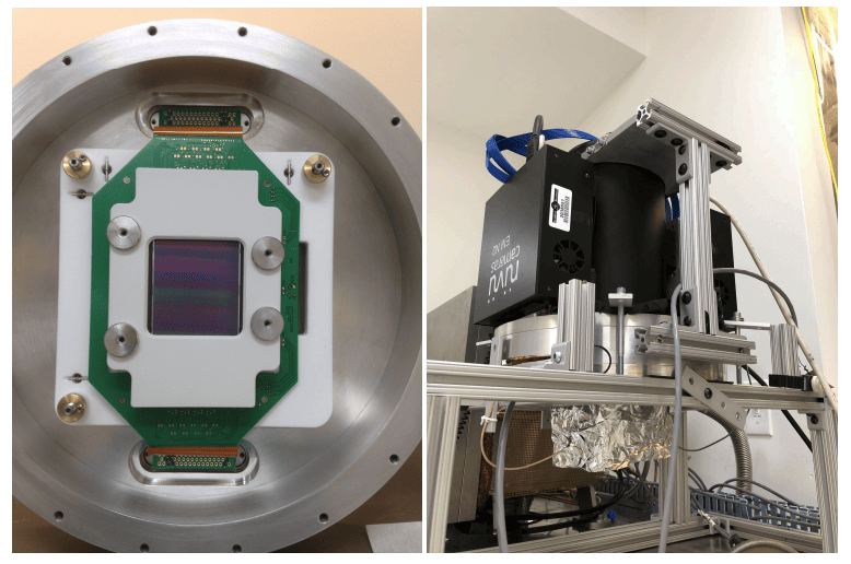
An engineering grade CCD282 lent by the Université de Montréal was installed in the LN2 cryostat (Section 3.2) and was characterized at Nüvü Camēras’ facilities. During the tests, the device was stabilized at −85◦C. This study did not explore other temperatures of operation.
For the reasons outlined in Section 3.1, the tests were performed at an horizontal frequency of 10 MHz. Two vertical frequencies were tested, 50 kHz, and 166 kHz, in both IMO and NIMO. In all cases, the horizontal clocks were kept identical.
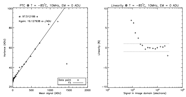
4.1 Read-out Noise and Vertical Full Well measurements
The Read-out Noise (RON) and Vertical Full Well (VFW) are measured by using the Photon Transfer Curve (PTC) method6 by shining a stabilized light source on the EMCCD while increasing the exposure time to vary the number of accumulated photons. The method yields at the same time the RON and the reciprocal gain of the system (k-gain), and the linearity can be inferred since the the change in the exposure time yields a linearly increasing signal. The RON and k-gain are related to the horizontal shifting and are therefore independent from the VFW if one assumes that the horizontal shifting capacity (e) will always be greater than the vertical shifting capacity. In the case of the CCD282, this is true for unity EM gain since the vertical and horizontal charge handling capacity of Teledyne-e2v EMCCDs are usually <100 ke, and >200 ke, respectively.
Figure 4 shows the PTC obtained on one output of the CCD282 in NIMO at a vertical shifting frequency of 50 kHz, an horizontal shifting frequency of 10 MHz, and a unity EM gain. The readout noise is ∼100 e, and the system’s k-gain is ∼19 e/ADU, which is similar to what is usually achieved with the CCD201-20 with the same kind of electronics. In those conditions, the VFW is ∼23 ke (∼1200 ADU). The linearity at low signal (below ∼10σ) is challenging to measure properly and the degradation towards 0-signal should not be considered a firm trend.
In IMO, it is expected that the achieved VFW is lower since there are no clocks that are held in a high state during the integration. In the case of the 50 kHz vertical clocks, the measured VFW is ∼12 ke.
When using vertical clocks that are close to the RC constant of the CCD, one can expect to achieve a lower FW since the clocks’ amplitude will be damped towards the center of the CCD. In the case of the CCD282, running the vertical clocks at 166 kHz yields a VFW of ∼20 ke in NIMO. In IMO, since the capacitance of the phases increase significantly, this further increases the damping effect. As a result, the measured VFW in IMO at 166 kHz is ∼8 ke.
4.2 Dark current and Clock Induced Charges measurement
By using the same read-out parameters as those used in Section 4.1, the device was put in complete darkness and the High Voltage (HV) clock of the EM registers were adjusted to yield an EM gain of 1000. Then, in order to disentangle the horizontal from the vertical CIC components, the device was read-out by overscanning in both the horizontal and vertical directions (same method as the one presented in [7]). The resulting images consist of 4 quadrants. The top left quadrant is the image area. It contains the total unwanted signal, which is the dark current accumulated in the image area during the integration, the dark current accumulated in the storage area during the read-out, the CIC generated during the image vertical shift, the CIC generated during the storage vertical shift, and the CIC generated by the horizontal shift. The bottom left quadrant is the vertical overscan. It contains the dark current generated in the storage area during the read-out, the CIC generated during the storage vertical shift, and the CIC generated by the horizontal shift. The right quadrants correspond to the horizontal overscan. They contain the CIC generated by the horizontal shift. Thus, the horizontal CIC can be obtained readily from the right quadrants. Finally, the total signal generated in the image domain during the read-out process (vertical CIC and dark current) can be derived by subtracting the horizontal CIC from the signal measured in the bottom left quadrant. From those data alone, it is not possible to perfectly disentangle the vertical CIC from the dark current, especially in NIMO. In this mode of operation, the dark current recovers only after a characteristic time when the phases are switched out of inversion.8, 9 As a result, the measured dark current in NIMO will be a function of the time the integration phases will be idle between the read-outs. For small CCDs, where the read-out time is short, it can be assumed that the dark current generated during the read-out process is negligible as compared to the vertical CIC. However, for the CCD282, the read-out is of the order of 0.25 s and this assumption can’t be made. For this reason, and since it is the total number of spurious charges generated (the total background signal) that matters, this paper will refer to the ”vertical signal” the sum of the vertical CIC and the dark current generated during the read-out process.
The Figure 5 shows the dark current and CIC measurements in both NIMO and IMO, for a vertical frequency of 166 kHz, and an horizontal frequency of 10 MHz at -85◦C. The top right panel of the figure shows the trend of the dark current that increases as a function of the integration time in NIMO, where it almost double (3.5 to 6·10-3 e/pix/s) from 1 to 64 seconds of integration. In IMO, the measured dark current is in excess of an order of magnitude lower, in the range of 1–2·10-4 e/pix/s, and, as expected, it shows no obvious trend with respect to the integration time.
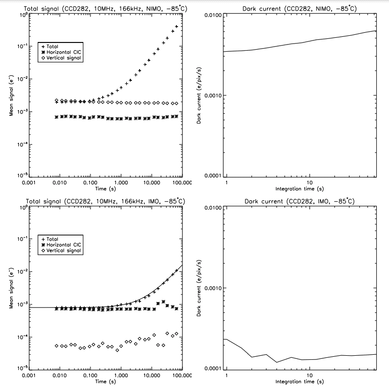
The CIC measurements (left panels of Figure 5) shows that the horizontal CIC is the same regardless of the operation mode, at about 7·10-4 e/pix/im, or 3.4·10-7 e/pix/transfer (the horizontal register is composed of 2080 elements).
Regarding the vertical signal, the NIMO clocking generates more charges since the dark current is higher as compared to the IMO. In those cases, the vertical clocks applied were sinusoidal, which was demonstrated to produce a level of CIC in IMO that is comparable to the one achieved in NIMO with similar clocks.10 In NIMO, the level of charges generated in the image domain is 1.9·10-3 e/pix/im. Assuming a dark current of 3.5·10-3 e/pix/s at the minimum integration time (top right panel of Figure 5), and a read-out time of 0.8 s (since the read-out does overscanning), one quickly realize that the vertical signal is completely dominated by the dark current, and the level of vertical CIC is negligible.
In IMO, the level of charges generated in the image domain is 6.7·10-5 e/pix/im. Assuming a dark current of 1.5·10-4 e/pix/s, for a read-out time of 0.8 s, the vertical signal can still be dominated by the dark current. However, if one would assume that the dark current is negligible, this would put a higher limit of 1.7·10-9 e/pix/transfer (the read-out of an entire image requires 4117 vertical shifts) to the vertical CIC. It is of importance to note that this level of CIC is achieved with the same clocks that has demonstrated a VFW of 8 ke in IMO (Section 4.1).
It might by argued that in order to yield a lower vertical background signal in NIMO, one could operate the EMCCD at a lower temperature. However, authors have measured an increasing level of horizontal smearing as an EMCCD operated at high EM gain is taken to colder temperatures.10, 11 One might think that this unwanted effect can be mitigated by altering the horizontal clocks, such as increasing their amplitude, but so far, this has not solved the case and horizontal smearing is still considered as being temperature-dependent.10, 12
As outlined in [4], by knowing both the dark current and CIC level of the NIMO and IMO, one can compute the maximum integration time at which it is preferable to use NIMO over IMO. In the case of the CCD282 clocked with sinusoidal vertical clocks, since the read-out is a long process, there is no integration time for which the total background signal of the NIMO is lower than IMO. Hence, in order to prevent horizontal smearing and get a low background signal, the operation of this EMCCD in IMO at a reasonable temperature should be preferred.
4.3 CTE measurements
It is of importance to assess the capability of the clocks to properly shift the electrons within the device. As a matter of fact, one can get a very low CIC (either vertical or horizontal) by reducing the amplitude of the clocks to very low levels. However, the charge transfer might then become ineffective and a high proportion of electrons will not be shifted at the right time. Moreover, regarding the vertical shift, clock of too low an amplitude might just not shift the charges at all. In this condition, the measurement of the vertical CIC will effectively yield very low numbers: the charges in the image domain do not make it to the horizontal register for being read-out. Hence the importance to assess the level of CIC together with the FW (as shown in the previous section) and Charge Transfer Efficiency (CTE).
It was shown in [13] that the vertical CTE is almost independent of the clock shape and amplitude when the achieved VFW is of the order of the maximum achievable VFW on the device. For this study, since the clocks used for measuring the CIC are generating a VFW that is close to the maximum of the device, it is expected that the vertical CTE is limited by the device itself rather than by the clocks.
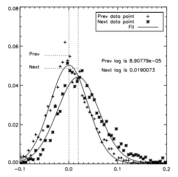
On the other hand, the horizontal CTE when the device is operated at a high EM gain can vary greatly regardless of the achieved FW. At high speed (10 MHz in this case), the timing of the HV clock with respect to the conventional clocks, the voltage and time at which the clocks overlaps, and the voltage on the RϕDC node are playing an important role in the CTE, and it is possible to achieve an acceptable FW together with a poor CTE. Thankfully, one can measure the horizontal CTE at high EM gain by measuring the signal of isolated bright pixels (assumed to contain either 1 electron of dark current or 1 electron of CIC) of dark frames with their immediate neighbouring pixel. The relative signal level of the neighbouring pixel gives the proportion of deferred charges from the bright pixel. By the following formulæ, the minimum and maximum CTE are then inferred:

where Pd is the proportion of deferred charges, nEM is the number of elements of the EM register, nCONV is the number of conventional elements of the register underneath the storage area, and nCONVe is the number of conventional elements in the extended horizontal register. In the case of the CCD282, these numbers are 600, 1040, and 440 respectively. The CTEmin boundary assumes that all of the Charge Transfer Inefficiency (CTI) comes from the EM register and the conventional registers shift charges perfectly, while the CTEmax boundary assumes that the CTI is spread equally across all of the horizontal register’s elements. In the case of the images used for this measurement, which contained solely dark current and CIC for integration time of up to 64 s, one knows that it is very unlikely that the conventional register will have more than one electron per pixel. Hence, in this regime, it is only the CTE of the EM register that is probed, and this value is given by CTEmin.
Figure 6 shows the results of of the horizontal CTE measurement. The ”Prev” data points is used as a reference and represents the relative intensity of the pixels before the bright ones. One would expect those pixels to have 0 signal, which is the case at a ∼10-4 relative intensity. The ”Next” data points represent the relative intensity of the pixels following a bright one; they are the ones used to measure the level of deferred charges. In the case of the CCD282 operated at -85◦C in IMO, and 10 MHz of pixel rate at an EM gain of 1000, the level of deferred charges is 1.9%, which translates to a CT Emin of 0.999968. The same level of deferred charges is measured with the NIMO read-out.
The advent of large-format EMCCDs opens a new frontier in optical spectroscopy and will not only enable new science, it will have an impact on how we conceive the spectrograph entirely. One could wonder why all observations with astronomical spectrographs are not obtained at the highest possible resolution and binned depending on which feature one wishes to measure. Generally speaking, this approach is impractical as binning high-resolution spectra rapidly increases the effective readout noise and renders high-resolution spectrograph inefficient compared to lowresolution spectrographs with proper pixel sampling. In this context, the noise properties of EMCCDs open new possibilities. State-of-the-art high-resolution cross-dispersed optical spectrographs cover the entire optical domain at a λ/∆λ resolution of 80 000 and more.14–16 Equipping such a spectrograph with an EMCCD would render it very versatile; while preserving the high-resolution capabilities, one could observe an object below the detection threshold per resolution element and bin the data in post-processing to a much lower resolution without paying the readout noise penalty generally associated with spectral binning. This could be particularly exciting for objects that have strong colour gradients. For example, ultracool L or T dwarfs have extremely red g − z colours; while one could observe the far-red domain (850-1000 µm) at full resolution while still obtaining valuable data in the optical domain at much reduced resolution. As resolution is determined in post-processing, one would maintain the capability of detecting narrow emission lines is such objects (e.g., Hα) while preserving SNR on large-scale, low-level, spectral structures.
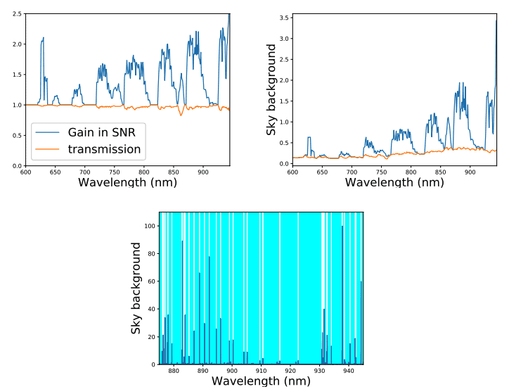
Low-resolution (λ/∆λ < 5 000) spectroscopy in the rizy bandpasses suffers from the additional background associated with OH sky lines. Higher resolution spectroscopy resolves these lines and can detect a faint continuum between lines, but this capability to separate OH lines from the science spectrum comes with a loss of sensitivity due the spreading of the target’s flux on a larger number of pixel that have their associated readout noise. In that context, a high-resolution spectrograph coupled with an EMCCD becomes interesting as one can mask OH lines prior to the binning in the post-processing. The decrease in the effective background per resolution element in the binned spectrum will lead to an increase in sensitivity compared to observations taken with a native resolution corresponding to the binned spectrum. Figure 7 illustrates the gains in observing at R = 20 000 with an EMCCD-equipped spectrograph binned to a resolution of 5 nm (R ∼ 150 in the far-red).
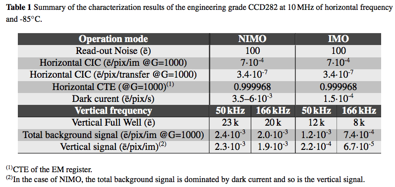
A summary of the characterization results of the 4k × 4k engineering grade CCD282 are presented in Table 1. The performance of the device in IMO at 166 kHz is outstanding: the level of vertical signal is an order of magnitude lower than what is achieved on the smaller CCD97 (512 × 512) with vertical clocks running ∼10 times slower on the CCD282 and the image requiring 4 times the vertical shifts to be read-out. Considering that the horizontal CIC is comparable to the CCD201- 20, the CCD282 sets a new standard and truly makes photon counting possible on this large area. With regards to the relation between the vertical clock frequency and the vertical CIC generation rate, the CCD282 follows the same trend as the other EMCCDs of Teledyne-e2v: the vertical CIC increases with slower vertical clocks, for both IMO and NIMO. On the other side of the spectrum, vertical clock speeds beyond the RC frequency were not tested but they could potentially reduce further the vertical CIC. Similarly, modifications to the CCCPv3 hardware were made to allow for clocking the horizontal registers at 15 MHz in order to reach a higher number of frames per second. The impact on the horizontal CIC will have to be measured.
One could argue that the low (8 ke) VFW achieved in this mode might be problematic, but one must remember that if the device is ought to be used in a regime where single photon counting is required, the EM register will saturate well before the pixel. As a result, it is not the pixel’s well that is the limiting factor to the dynamic range. Moreover, since the cost of the read-out with an EMCCD is essentially nil once the accumulated dark current reaches a level that is comparable to the total CIC, the dynamic range can be broadened by means of more numerous read-outs with little impact on the SNR at low flux.17
The architecture of the CCD282 renders necessary the assessment of the gain matching between each outputs. Not only does the output amplifier’s response can vary from one output to another, but the EM gain calibration (the relation between the HV clock amplitude and achieved EM gain) does differ. Moreover, since a single HV clock is responsible for the EM process of two adjacent outputs, it is not be possible to correct for inconsistencies in the EM gain process of those two outputs. Even though the EM gain process should be well matched as the two register are in close proximity to one another on the die, to some extent there will be differences that have to be characterized. Through this study, and even though it is an engineering grade detector that was used, data was gathered that shows a pretty good match between the outputs, but more data, and more specifically data from a scientific grade detector, is required to fully characterize their behaviour.
The video chains of the controllers used for the characterization were based on those used for the CCD60, CCD97, and CCD201-20. However, since the CCD282 exhibits an overspill drain that limits the number of charges generated in the EM register to ∼200 ke with the DC levels used, the gain of those chains could be increased to yield a higher response, a better use of the ADC dynamic range, and perhaps a lower read-out noise. Moreover, since the VFW is lower than the other devices, this change would not have an impact on the saturation point of the pixels.
This paper presented the preliminary characterization results of the CCD282 clock with two CCCPv3 controllers from Nüvü Camēras. The results shows that although the device is much larger than those who have been extensively studied in the past, the level of background signal (dark current + CIC <10-3 e/pix/im) is very low and it is well adapted to photon starved and photon counting applications, even when operated in IMO. The low dark current generated by this mode of operation (1.5·10-4 e/pix/s) makes it best suited for use in high resolution spectroscopy applications, where the continuum of the sky background is almost inexistent for some spectral bins, and long (few to several seconds) integrations will be beneficial. The low background signal is partly due to the design choices that were made, namely to lower the pixel’s well to make it possible to use vertical clocks of a lesser amplitude. Even though the pixel’s well is noticeably lower on the CCD282 (8–25 ke depending on the operation mode and vertical clock frequencies) than what is usually seen in CCDs, other aspects of the device (low read-out noise, high frame rate) make it possible to easily overcome this limitation. The implementation of an overspill drain in the EM register is a good addition to the EMCCDs since it prevents the cosmic rays from flooding the multiplication register. Eventually, this should also slow or prevent EM gain ageing, although is was not measured in this study.
This large format EMCCD is of interest for astronomical applications requiring a high sensitivity, whose mean fluxes ranges from a fraction of a photon to several tens per pixel per frame, up to moderate frame rate, over a large field of view. High resolution spectroscopy, with the added benefits of noise-free spectral binning and sky spectrum removal, wide field photometric surveys, transient objects and orbital debris monitoring and identification are some applications that will benefit from such a detector.
Acknowledgments
Nüvü Camēras is grateful to the Canadian Space Agency for funding this study under the STDP AO-4.
1 P. Jerram, P. J. Pool, R. Bell, et al., “The LLCCD: low-light imaging without the need for an intensifier,” in Sensors and Camera Systems for Scientific, Industrial, and Digital Photography Applications II, M. M. Blouke, J. Canosa, and N. Sampat, Eds., Proc. SPIE 4306, 178–186 (2001).
2 J. Hynecek, “Impactron-a new solid state image intensifier,” IEEE Transactions on Electron Devices 48, 2238–2241 (2001).
3 D. Jordan and P. Jorden, “A Novel 4k x 4k EMCCD Sensor for Scientific Use,” in Scientific Detectors Workshop Proceedings, (2013). 4 “Low-light Technical Note
4 Dark Signal and Clock-Induced Charge in L3Vision CCD Sensors,” tech. rep., E2V Technologies, http://www.e2v.com/content/uploads/ 2015/04/a1a-low-light_tn4_3_v1.pdf (2004).
5 O. Daigle, P.-O. Quirion, and S. Lessard, “The darkest EMCCD ever,” in Society of PhotoOptical Instrumentation Engineers (SPIE) Conference Series, Society of Photo-Optical Instrumentation Engineers (SPIE) Conference Series 7742 (2010).
6 J. R. Janesick, Scientific charge-coupled devices, Scientific charge-coupled devices, Bellingham, WA: SPIE Optical Engineering Press, 2001, xvi, 906 p. SPIE Press monograph, PM 83. ISBN 0819436984 (2001).
7 O. Daigle, O. Djazovski, D. Laurin, et al., “Characterization results of EMCCDs for extreme low-light imaging,” in Society of Photo-Optical Instrumentation Engineers (SPIE) Conference Series, Society of Photo-Optical Instrumentation Engineers (SPIE) Conference Series 8453 (2012).
8 P. Jorden, P. Pool, and S. Tulloch, “Secrets of E2V Technologies CCDs (ex Marconi CCDs),” Experimental Astronomy 14, 69–75 (2002).
9 B. Burke and S. Gajar, “Dynamic suppression of interface-state dark current in buriedchannel CCDs,” Electron Devices, IEEE Transactions on 38, 285 –290 (1991).
10 E. T. Hamden, N. Lingner, G. Kyne, et al., “Noise and dark performance for FIREBall-2 EMCCD delta-doped CCD detector,” in UV, X-Ray, and Gamma-Ray Space Instrumentation for Astronomy XIX, Proc. SPIE 9601, 96010O–96010O–10 (2015).
11 O. Daigle, C. Carignan, J. Gach, et al., “Extreme Faint Flux Imaging with an EMCCD,” Publications of the Astronomical Society of the Pacific 121, 866–884 (2009).
12 L. K. Harding, R. T. Demers, M. Hoenk, et al., “Technology advancement of the CCD201- 20 EMCCD for the WFIRST coronagraph instrument: sensor characterization and radiation damage,” Journal of Astronomical Telescopes, Instruments, and Systems 2(1), 011007 (2015).
13 O. Daigle, O. Djazovski, M. Francoeur, et al., “EMCCDs: 10 MHz and beyond,” in High Energy, Optical, and Infrared Detectors for Astronomy VI, Proc. SPIE 9154, 91540B (2014).
14 S. S. Vogt, S. L. Allen, B. C. Bigelow, et al., “HIRES: the high-resolution echelle spectrometer on the Keck 10-m Telescope,” Proc.SPIE 2198, 2198 – 2198 – 14 (1994).
15 J. Ge, J. R. P. Angel, B. Jacobsen, et al., “An Optical Ultrahigh-Resolution Cross-dispersed Echelle Spectrograph with Adaptive Optics,” Publications of the Astronomical Society of the Pacific 114, 879–891 (2002).
16 H. Dekker, S. D’Odorico, A. Kaufer, et al., “Design, construction, and performance of UVES, the echelle spectrograph for the UT2 Kueyen Telescope at the ESO Paranal Observatory,” Proc.SPIE 4008, 4008 – 4008 – 12 (2000).
17 O. Daigle, O. Djazovski, J. Dupuis, et al., “Astronomical imaging with EMCCDs using long exposures,” in Society of Photo-Optical Instrumentation Engineers (SPIE) Conference Series, Society of Photo-Optical Instrumentation Engineers (SPIE) Conference Series 9154, 0 (2014).