The rapid proliferation of Electron Multiplying Charge Coupled Devices (EMCCDs) in recent years has revolutionized low light imaging applications. EMCCDs in particular show promise to enable the construction of versatile space astronomy instruments while space-based observations enable unique capabilities such as high-speed accurate photometry due to reduced sky background and the absence of atmospheric scintillation. The Canadian Space Agency is supporting innovation in EMCCD technology by increasing its Technology Readiness Level (TRL) aimed at reducing risk, cost, size and development time of instruments for future space missions. This paper will describe the advantages of EMCCDs compared to alternative low light imaging technologies. We will discuss the specific issues associated with using EMCCDs for high-speed photon counting applications in astronomy. We will show that a careful design provided by the CCD Controller for Counting Photons (CCCP) makes it possible to operate the EMCCD devices at rates in excess of 10 MHz, and that levels of clock induced charge and dark current are dramatically lower than those experienced with commercial cameras. The results of laboratory characterization and examples of astronomical images obtained with EMCCD cameras will be presented. Issues of radiation tolerance, charge transfer efficiency at low signal levels and lifetime effects on the electron-multiplication gain will be discussed in the context of potential space applications.
Scientific low light imaging applications such as astronomical spectroscopy, faint object photometry, coastal surveillance and molecular imaging drive optical sensor system requirements towards the detection of ever smaller signals at increasing pixel rates. Since their invention in 1969, the Charge-Coupled Devices (CCDs) have become the detector of choice for high quality low light imaging in a wide range of fields. They have the advantages of excellent resolution, 100% fill factor, greater than 90% peak quantum efficiency, excellent charge transfer efficiency and very low dark signal with sufficient cooling.1 However, the performance of conventional CCDs has always been limited by readout noise inherent in the output amplifier of the device. To minimize read noise the readout speed has to be relatively slow in the order of a few seconds to read the image. In the electron multiplying CCD (EMCCD) device technology developed in the 1990s an additional gain register is incorporated in the architecture through which the signal passes as it is read out of the CCD array.2 Because the signal is amplified prior to readout this effectively reduces the magnitude of the amplifier noise and improves significantly the signal-to-noise ratio (SNR) without restrictions of slow readout times. In addition to all advantages of the CCD technology, EMCCDs are able to achieve sub-electron read noise at high frame rates allowing single-photon detection. 3,4 The EMCCDs are now available commercially from E2V Technologies Ltd. and from Texas Instruments. In spite of the reported improvements in performance, the EMCCDs have not been widely used in space instrumentation. In this paper we review the advantages of EMCCDs in comparison alternative low light imagers and discuss the specific issues relating to their operation and potential applications. The results of laboratory characterization and astronomical testing are presented to demonstrate the superior performance of this low light imaging technology.
2.1. Scientific CCDs
The state-of –the-art scientific-grade CCDs are available in a number of distinct technologies such as front-illuminated CCDs, thinned back-illuminated CCDs and back-illuminated deep-depletion CCDs. In a traditional front-illuminated CCD light passes through the polysilicon gates that define each pixel and generates electric charge in the collecting well when pixels are electrically biased. Due to reflection and absorption losses in the poly-gate structure quantum efficiency (QE) of front-illuminated devices is only about 50%. To improve QE, the Si substrate material can be uniformly removed to attain approximately 10 to 15 μm thickness so that an image can be focused directly onto the photosensitive area of the CCD without absorption losses in the gate structure. Compared to front-illuminated CCDs, these thinned back-illuminated devices have a higher QE across the visible spectrum with peak QE >90%. To further improve QE, especially for near-infrared (NIR) imaging and x-ray applications, the CCD are manufactured from a high-resistivity silicon with a thickness ranging from 50 to 300 μm in order to produce a “deeper” depletion region (i.e., larger active photosensitive volume). This architecture allows longer-wavelength photons to interact within the depletion region layer as opposed to merely penetrating it, ultimately helping to increase QE in the NIR spectral region
Some back-illuminated CCDs have specifically been designed for low-light detection in scientific applications.1 They offer the advantages of highest QE over a broad spectral region, excellent resolution, and possibility to achieve a very low dark signal with sufficient cooling. However, they suffer from noise inherent in the process of reading out the signal. Even in the best devices, this is typically 2 - 4 electrons RMS with a slow readout rate (several seconds to read the entire chip) and much more if the readout amplifier bandwidth is increased to give a fast readout.
2.2. Intensified CCDs (ICCDs)
The readout noise limitation can be eliminated by enhancing the light level before it reaches the CCD. In an intensified camera (ICCD), a vacuum tube image intensifier is fiber-optically coupled to the CCD chip to enhance its sensitivity down to a single photon level. The photon multipliers consist of three main components: a photocathode, a microchannel plate (MCP) and a phosphor screen. The light is focused onto a light-sensitive photocathode and the resulting photoelectrons directed into an electron multiplier and then multiplied to a number dependent on the gain voltage (hundreds of volts) before hitting a phosphor screen to give a much larger number of photons than the original flux. The phosphor screen is coupled to the CCD by a fiber optic bundle and the resultant signal is sufficiently high that the background noise becomes insignificant. Single photons can be detected and discriminated from CCD noise and ultra high-speed phenomena can be captured by using the image intensifier with fast gating function.
Disadvantages of ICCDs include larger physical size, lower resolution compared to a non-intensified camera with the same CCD chip (MCP and phosphor make a major contribution to degrading the MTF of a CCD), lower QE than that of a bare CCD and additional noise sources associated with thermonic emission from the photocathode and statistical variations inherent to the electron gain mechanism.5 The vacuum tube intensifier has limited life and is easily damaged. In addition, high voltage in the range of 600 to 900 V required to set the gain of the MCP makes the control circuitry prone to reliability concerns in space environment.
2.3. Electron Multiplying CCDs (EMCCDs)
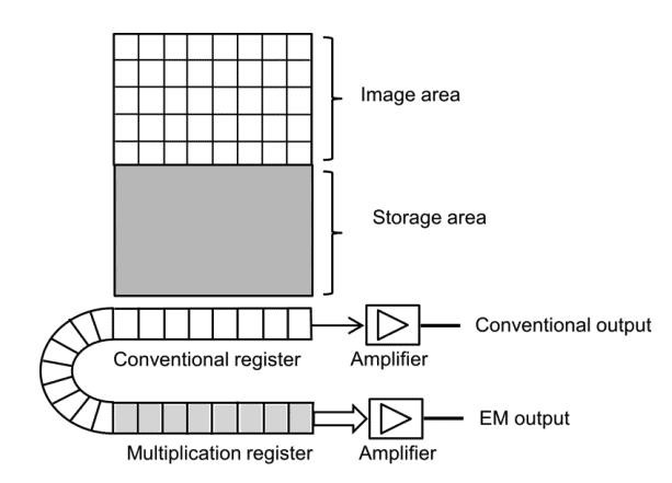
About ten years ago, EMCCDs became commercially available. EMCCD sensors are similar to conventional CCDs but with an additional multiplication register operated at a high clock voltage which amplifies the signal between the end of the conventional serial register and the output amplifier as shown in Fig. 1. By using clock voltages in the 30-50 V range rather than the more common 10 V, electrons are accelerated on passing through the cells of multiplication register and have a small probability (up to 2%) of generating a second electron by avalanche multiplication. Although the statistical gain is small, after passing through several hundred multiplication stages the overall gain of several hundred to several thousand can be achieved. The readout noise caused by the output amplifier is effectively divided by this overall gain yielding net readout noises of a tiny fraction of one electron. By eliminating readout noise the EMCCDs represent a major enhancement of CCD performance while retaining all advantages of conventional CCDs such as high quantum efficiency and charge transfer efficiency, low dark current, cosmetic quality and manufacturability.
2.4. CMOS Sensors
CCD and CMOS sensors were both developed in the late 1960s. However, CCDs became dominant in the imaging sensors market until the 1990s because they produced better image quality with the manufacturing technology available. CMOS sensors have required better uniformity and smaller feature sizes that wafer fabrication plants have been able to achieve with the development of advanced lithography processes. Currently both CCD and CMOS sensors offer excellent imaging performance. In addition, CMOS sensors offer more functionality such as timing and control electronics, signal processing electronics, analog to digital converter and digital interface integrated on one chip. This allows to achieve a cost-effective, highly integrated and compact imaging system known as a camera-on-a-chip which has evolved dramatically in recent years in consumer electronics and industrial applications. State-of-the-art scientific CMOS devices with hybrid architecture are available in formats as large as 4Kx4K four-side buttable that is essential for making large FPA mosaics and radiation tolerant by design. CMOS detectors have very low power consumption and allow non-destructive random access to the pixels and on-chip integration of analog and digital circuitry which significantly reduces the imaging system mass, volume, power and thermal output and overall complexity for space use. 6
CMOS sensors have already been used in space in satellite bus instrumentation such as star trackers and inspection systems. The photon counting imager for the Ultra Violet Imaging Telescope (UVIT) of ASTROSAT mission has been developed in Canada using an intensified CMOS detector.7 Although state-of-the-art scientific CMOS sensors have demonstrated outstanding characteristics and imaging performance the CMOS technology is yet to have a significant impact in scientific payloads for which the mature CCD technology remains dominant. Specifically, the CCDs remain unchallenged in dynamic range and photometric accuracy while EMCCDs have a number of distinct advantages for photon counting applications. 3 Scientific CMOS sensors will definitely play an increasing role in space instrumentation especially in systems with size, mass and power constraints, operation scenarios requiring windowing modes and random pixel access as well as for space missions requiring enhanced radiation tolerance.
3.1. Noise Sources in CCDs
The key parameter for evaluating sensor performance under low-light imaging conditions is the signal-to-noise ratio (SNR). Two fundamental characteristics system noise and quantum efficiency determine the sensitivity of any imaging camera system. QE specification is one of the most important parameters during the camera system design. However, in many cases the system noise is the key factor affecting the overall image quality. A calculation of SNR is based on its definition, i.e. detected signal S = P QE t, where P is the number of photons incident on a pixel, QE is the quantum efficiency of the CCD divided by the detector system noise which combines the principal sources using the ‘root of sum of squares’ law as follows:

where the term √(P QE t) represents the shot noise associated with the statistical variation in the arrival rate of photons incident on the CCD. Since the interval between arrival of individual photons is governed by Poisson statistics the photon shot noise is equivalent to the square root of the signal. While the shot noise will increase with increasing signal intensity the SNR will improve also.
DN is the dark noise associated with the statistical variation in the number of electrons thermally generated within the silicon structure of the CCD which is independent of photon induced signal, but highly dependent on device temperature. The rate of generation of thermal electrons at a given CCD temperature is termed dark current. In similarity to shot noise, dark noise follows a Poisson relationship to dark current and is equivalent to the square root of the number of thermal electrons generated within the image exposure time.
RN is the read noise which is a combination of system noise components inherent to the process of converting CCD charge carriers into a voltage signal for quantification and the subsequent processing and analog-to-digital conversion. The major contribution to read noise usually originates with the on chip amplifier, and this noise is added uniformly to every image pixel.
The shot noise contribution is reduced by using device design and manufacturing techniques such as CCD back-thinning to ensure that the QE as high as possible and then at camera system level by taking a sufficiently long exposure. Dark current is minimized significantly with effective cooling inherent to most high-end scientific CCD cameras, and even during use of moderately long exposures it may often be considered practically negligible relative to the read noise. Therefore, the most significant source of noise is the read noise. In a conventional CCD a read noise of 2 - 4 electrons RMS can be obtained at the expense of a slow readout time of several seconds.
3.2. Noise Considerations for EMCCDs
The major advantage of the EMCCD technology is that electron multiplying gains can be sufficient to effectively reduce readout noise to negligible levels even at high readout rates eliminating this primary contributor to the detection limit of an imaging system. Therefore, the RN term can be removed from the SNR equation. The gain mechanism amplifies the signal prior to the output amplifier, therefore an additional term G (gain factor) will appear in the SNR equation for EMCCD. In addition, noise in the electron multiplication gain contributes and excess noise factor (ENF) as shown in Equation 2.

The ENF is present in all signal amplifying technologies such as EMCCDs or ICCDs and is related to a statistical variation in the overall number of electrons generated from an initial charge packet by the signal multiplying process. Thus, there exists a small probability that the impact ionization will produce an extra electron during each transfer of electrons from element to element along the gain register. Although this probability is small but when executed over a few hundred of steps, very large potential gains may result. The results of theoretical and experimental work has identified ENF at a value of √2 , or 1.41 for EMCCD technology while Multi-Channel Plate (MCP) and ICCDs have noise factors typically ranging from 1.5 to >2.
In EMCCDs the dark noise is amplified by the gain register and represents the dominant form of noise in the device. It consists of two components: the thermal noise and the clock induced charge (CIC). The thermal component of the dark signal: can be reduced by cooling the device and by employing an inverted mode of operation (IMO). The CIC is generated by the clocking process which moves the signal from one cell to the next during readout and can be minimized by precise control over clocking parameters.
4.1. Cooling
Cooling a CCD greatly reduces the dark current. For example, a non-cooled CCD might generate a dark current of 300 e/s/pixel at 20°C, but only 1 e/s/pixel at -40°C. While most scientific CCDs have traditionally been cooled to around -50ºC, in the particular case of EMCCD cameras, deep cooling down to -85°C or lower is needed to minimize the thermal noise to an insignificant level. In addition, it is important to provide accurate temperature stabilization because the gain is also temperature dependent. In order to obtain this degree of cooling it is necessary to house the chip in a hermetically sealed, evacuated enclosure. These engineering requirements and advanced packaging have led to an improvement in reliability of EMCCD cameras in comparison to conventional CCD cameras, however their cost has increased substantially.
4.2. Clocking modes
Two clocking modes called non-inverted and inverted clocking can be used to clock CCDs and many performance parameters such as dark current generation, spurious charge and residual image are highly dependent on clocking mode.1 In CCDs dark current is caused by thermally generated electrons in the silicon. It has two components, the surfacegenerated component associated with Si-SiO2 interface states and the bulk component associated with carrier generation in the depletion and field-free regions of the device. The generation rate of the surface dark current depends on both the density of surface states and the density of free carriers (holes and electrons) at the interface. When an EMCCD is operated in non-inverted mode (NIMO), clocks applied to image section are positive. Under this condition signal channel and Si-SiO2 interface states are depleted of free carriers that enhances generation of dark current. Surface dark current varies greatly among different CCD manufacturers, depending upon the wafer fabrication processing being typically two orders greater than the bulk dark current.
Operation of the CCD in an inverted mode operation (IMO) eliminates the surface dark current because the clock voltages are driven more negative inverting the signal carrying channel and causing minority carriers (holes) to migrate and populate the silicon-silicon dioxide interface. However, this reduction in dark current is accompanied by a reduction in full well capacity. Advanced IMO (AIMO) device architecture developed by the E2v company minimizes this loss in full well capacity to typically 66% of that of a standard mode device.8 Both IMO or AIMO devices are generally used when medium to long integration times are required at high to medium temperatures, in systems with no cooler or a thermo-electric cooler.
4.3. Clock Induced Charge (CIC)
Another source of noise that must be taken into account even under conditions of short exposure times is Clock Induced Charge (CIC). CIC is a well-known phenomenon,1 and describes the generation of spurious single electron background events during the vertical transfer of charge. In addition, CIC events may be induced in the gain register of EMCCD sensors. CIC is usually ignored in conventional CCDs because these single electron events are normally lost within the read noise floor. However, in the EMCCD these single electron events are amplified by the gain register just as a photoelectron. Therefore, CIC can be considered as the true detection limit at the single photon detection level because a single photon will be indistinguishable from a CIC spike. At the EMCCD device level CIC can be reduced by specialized design considerations and advanced manufacturing processes while at the camera system level specialized high-resolution clocking parameters enable to minimize this source of noise. Of critical importance in CIC minimization is the ability to conduct fast vertical shifts when reading out the sensor.
4.4. Precision voltage clock timing
The key to maximizing performance advantages of the EMCCD technology is to carefully control the charge transfer process in order to ensure good charge transfer efficiency (CTE) and minimize CIC. This can be achieved by lowering the operating temperature of the EMCCD to about -85ºC because the amount of voltage required to shift charge between pixels in the multiplication register is proportional to the operating temperature. Although the deep-cooling approach is valid and has been used by some EMCCD camera manufacturers to control the pixels’ voltage clocks more easily, the precision voltage-clock timing is an essential component of a new generation of EMCCD imaging platform that delivers significantly improved key performance characteristics. In general, the basic architecture of an EMCCD controller is similar to a conventional slow scan CCD system and consists of a timing core which generates clock waveforms and controls a double correlated sampling signal chain and an analog to digital converter (ADC) which transfers the data from an output system to the host computer. The timing of the various operations must be precisely controlled to achieve best noise performance and the clock waveforms have to be carefully optimized to achieve the best image quality. However, the approach to designing a high-speed EMCCD controller with precision timing of clocks is quite different from that used for slow scan systems employing conventional CCDs. The pixel rates at which the performance of the CCDs are specified vary from 10MHz up to 35MHz (for different EMCCD devices) and there is a trend to increase the pixel rates as high as possible since the devices are being used for high-speed applications. Therefore, a big challenge is to develop the ability to control and adjust timings to less than 1 ns in repeatable and reproducible way. The design of clock driver circuits operating at these speeds is another challenge because the clock driver has to produce a fast enough edge but without compromising charge transfer efficiency due to ringing and generating CIC. Also, high-speed systems require careful thermal management at component, subsystem and system level and appropriate protection design due to high power dissipation.
All test data and imaging results described in this paper have been obtained with an EMCCD camera employing scientific-grade EMCCD devices from E2V Technologies and CCD Controller for Counting Photons (CCCP) manufactured by Nuvu Cameras.9 The CCCP controller generates the clocks and biases with precision timing, allows the digitization of the CCD output signal and includes a communication interface to transfer pixel’s data to an acquisition computer. The controller has been optimized for running an EMCCD at high speed with the specific design goal to reduce the CIC generated during the readout. CIC levels as low as 0.001 – 0.0018 event per pixel per frame (as opposed to per transfer) were measured on the 512 x 512 CCD97 EMCCD from E2V Technologies operating in inverted mode (as opposed to non-inverted mode). In addition, by using the arbitrary clock generators, it was possible to investigate the impact of the clock shape on the CIC generated during the read-out process.
Three devices CCD60 (128x128 FT), CCD97 (512x512FT) and CCD201-20 (1024x1024 FT) have been characterized in the camera system employing the CCD Controller for Counting Photons (CCCP). The experimental techniques and data analysis methodologies have been discussed in details elsewhere.10
5.1. Charge transfer efficiency
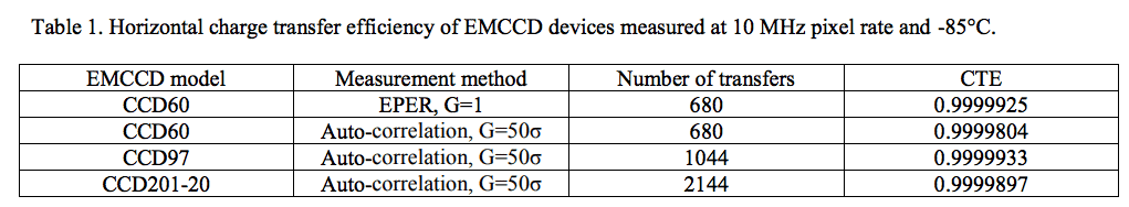
The horizontal charge transfer efficiency of the CCD60 device was measured by the extended pixel edge response (EPER) method.1 Flat-fields were taken with moderate (>10 ke/pixel) illumination and the deferred charges were measured in an overscan region. Due to the different device architecture the EPER method was not used for the CCD97 and CCD201-20 devices and their CTE was measured using the horizontal auto-correlation technique.10 The measurements were taken at an EM gain of 50. It should be noted that both the EPER and auto-correlation methods do not differentiate the CTE of the horizontal register from the CTE of the multiplication register. The results summarized in Table 1 show that all devices have excellent CTE when operated at 10MHz pixel rates.
5.2. CIC
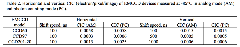
The results of earlier work9 have demonstrated that by using the CCCP to clock a CCD97 in IMO, the CIC generated by the vertical shift of the charges can be reduced to a very low level of 0.0005 e/pixel/image. During this study the vertical and horizontal CIC were measured for the CCD60, CCD97, and CCD201-20. In order to differentiate the horizontal CIC components from the vertical ones, the CCDs were overscanned in both the horizontal and vertical directions. For each CCD, 1000 dark images of zero integration time were taken at high EM gain (G/σ=50). The image processing methodology has been described before.10 Table 2 presents the results of measurements of horizontal and vertical CIC for different shift speeds. The results show that for all three CCDs operated with high EM gain the CIC generated during the horizontal shift is the dominant component. The use of lower EM gains reduces horizontal CIC, but not to the levels below the vertical CIC values. For example, at G/σ ratio of 5, the horizontal CIC (computed in AM) of the CCD201-20 is 0.0007 e/pixel/image.
5.3. Inverted mode (IMO) and non inverted (NIMO) operation modes
As discussed in Sec. 4.2 operation of an EMCCD in NIMO mode generates about 30 times less CIC than in IMO. Therefore, the optimum operating conditions of an EMCCD depend on integration time. Short integration times will benefit from the lower CIC achieved with the NIMO while long integration times will benefit from the lower dark current achieved with the IMO mode. As a compromise, switching the clocks between inverted and non-inverted modes during the integration would allow the CCD to operate below the characteristic time constant of the surface dark current generation that would reduce significantly this dark signal component. For short integration times, the read-out of the CCD has the same dithering effect, as the parallel clocks are being switched during this process. Based on the results of CIC characterization presented in the previous section we have concluded that the CIC was dominated by its horizontal component. Thus, the NIMO operation of the CCD would result in a minor advantage over IMO. In order to get more insight into optimum operating conditions of our EMCCD-controller system we have characterized the total background signal of the EMCCDs as a function of the integration time, temperature, and operating mode.
5.4. Total background signal
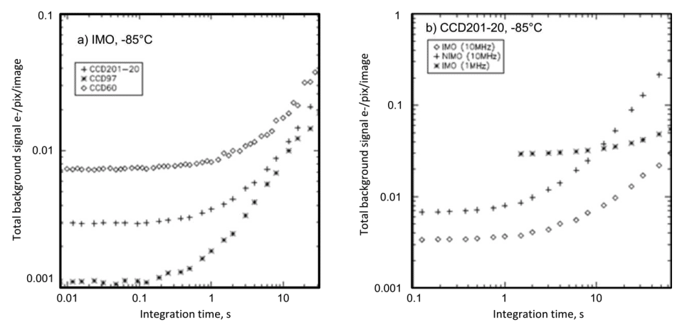
The total background signal is the most important parameter for low light imaging as it represents the sum of CIC and dark current. Thus, the plot of the total background signal per pixel per image as a function of the integration time will indicate the optimum operating conditions for a given integration time. Figure 2 a) shows that the mean background signal measured in IMO as a function of the integration time exhibits the CIC-dominated plateau at short integration times followed by the dark current-dominant region for longer integration times. At -85°C the dark current dominates the CIC for integrations longer than 5 s. The idea of driving the CCDs in NIMO to decrease the vertical CIC at the expenses of a higher dark current was tested using the CCD201-20 device. The solid and dotted lines of Figure 2 b) depict the total background signal as a function of the integration time for the IMO and NIMO operations at 10 MHz. During these measurements, the high and low levels of vertical clocks were modified to make the CCD operate in either IMO or NIMO while the same clock pattern was used for the horizontal clocking. The results show that, the total background signal of the NIMO operation is always higher than that of the IMO operation at all integration times used in the experiment. The CCD201-20 was also clocked horizontally at 1MHz in IMO (dashed line in Figure 2). While the dark current was about the same as with 10 MHz pixel rates, the amount of CIC generated in the horizontal register was dramatically higher (0.03 e/pixel/image), even though the EM gain required to get a G/ϭ ratio of 50 was lower due to reduced read-out noise level. On the basis of these results we have concluded that measurements of very low light level will benefit from operation of the EMCCDs at high speed that reduces the impact of horizontal CIC.
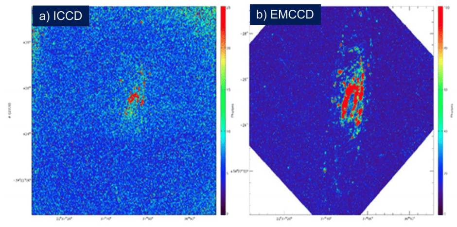
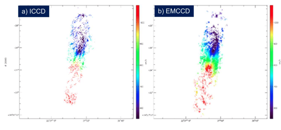
We have tested the EMCCD camera on the 1.6 meter Optical Telescope of the Observatoire du Mont Megantic to perform high resolution integral field spectroscopy of nearby galaxies at H-alpha. The EMN2 camera was mounted at the focal plane of the FaNTOmM integral field spectrograph. The FaNTOmM instrument consists of a focal reducer (F/2) and narrow band interference filter coupled to a high resolution (R15000) Fabry-Perot interferometer. Because FP interferometer is a scanning instrument it was important to scan the interferometer many times through the region of interest to account for photometric variations of the sky. This regime requires many short exposures (5-15 seconds between the moves of interferometer). The interferometer can be scanned rapidly (5 seconds per channel, 4 minutes per cycle of 48 channels) and the resulting images can be co-added and processed off-line to produce the final data cube. One of the typical applications of the FaNTOmM instrument is to study the kinematics of galaxies using the Doppler shift of the H-alpha line. The H-alpha emission originates from both very bright star forming regions (HII-regions) and faint diffuse H-alpha regions. The galaxy NGC7731 was chosen as one of the priority targets for this study, because it was studied extensively before3 with an ICCD camera allowing for a comparison of the two technologies. The EMN2 camera was used in both the analog and photon counting modes. In AM a single exposure of 5 seconds was taken between every move of the FP interferometer. In PC 10 exposures of 0.5 s were taken between every move of the interferometer, Thus, the total integration time between every move of the FP interferometer was constant. For every run dark frames were taken at the beginning and the end of the observation. All data cubes were processed with the data reduction techniques described by Diagle.11
It is important to note that in its standard configuration the FaNTOmM instrument employs an ICCD imaging device camera with GaAs photocathode and high speed CCD camera. Therefore, the objective of the test was twofold to determine if we can improve the image quality by using the EMCCD camera and if we can improve the science return of astronomical observations. Figures 3 and 4 show the monochromatic intensity maps (MI) and radial velocity maps of all observations. Qualitatively it is clear that under condition of similar integration times the galaxy’s approaching side is barely visible on the MI map obtained with the ICCD (Fig. 3a) while it appears well-resolved on the MI map obtained with EMCCD. (Figs. 3b). The RV map (Fig. 4a) shows only a few sparse pixels from this side of the galaxy that may result in large uncertainty in determination of the rotation velocity of this side of the galaxy. In contrast, the EMCCD map (Figs. 4b) provide much better data quality. Pixel by pixel comparison has shown that the same SNR was achieved 5 times faster with CCCP/CCD97 than with ICCD. Thus for the same integration time the CCCP/CCD97 data reveals a wider and more precise radial velocity field. It should be emphasized that for a true quantitative comparison between ICCD and EMCCD technologies more realistic experimental conditions must be considered. However, these first results are very encouraging and more astronomical data obtained with the EMCCD camera will be published soon.
7.1. Space Environment
Space instruments are continually bombarded by energetic plasmas, particles, and other forms of radiation from the sun and galactic sources. Of particular concern for spacecraft electro-optical systems engineers are total-ionizing-dose (TID) damage and single-event upsets (SEUs). The TID represents the cumulative effect of many particles hitting a device throughout the course of its mission life. The risk of component performance degradation can be mitigated through selection of radiation tolerant materials for the required mission, specialized manufacturing processes and technologies. Another approach known as radiation hardening by design (RHBD) relies solely on device design techniques to mitigate the damage caused by space radiation. The SEUs occur when high-energy particles penetrate the into materials and components generating excess charge. These effects can be managed at the imaging system level by using cosmic ray rejection algorithms and advanced readout schemes.
7.2. Reliability
To assure the reliability of the space mission, a program is needed to demonstrate that the detector technology has reached the maturity consistent with the Technology Readiness Level 6 (TRL 6) by the completion of program design phase. Requirements of the space environment as well as the physics of failure of the components must be analyzed and then, the critical parameters for each component in the FPA subsystem and acceptable deviation of those parameters can be established. After that the critical parameters will need to be evaluated for tolerance against environmental induced changes such as contamination, vacuum exposure, outgassing, launch vibration, thermal changes and radiation exposure. On this basis an efficient and effective testing plan will be developed that qualifies a component to a specific criteria defined by the program given the mission requirements and the component limitations. Because there are usually no space-qualified detectors for electro-optical systems available and higher performance commercial technology is used in the detector systems the common approach to qualification of commercial-off-the-shelf components (COTS) for space environments developed by the NASA Parts and Packaging Program12 can be used for qualification of detector systems.
From the considerations of device architecture it follows that EMCCD should behave in the same way as conventional CCDs in terms of operational changes resulting from radiation damage to the imaging area of the device, as there is no difference in construction. The main concern about using EMCCDs in the space radiation environment was the possibility of defect generation in the high field region of a gain register as a result of displacement damage. Such a defect could inject electrons into the pixel which, although at a low level, would then be amplified during transfer through the gain register. However, the results of testing of 94 EMCCDs to a 10 MeV equivalent fluence of 2 x 10¹⁰ protons/cm-2 carried out for the Gaia mission13 resulted in no device failures and the characteristic gain profile of each device has not shown any significant change after irradiation. This work has greatly improved confidence that EMCCDs can be used in space with a very low risk of catastrophic failure.
7.3. Detector Packaging
Packages for the scientific detectors are vacuum-sealed enclosures in which the sensor chip is mounted and maintained at required operating temperature. Since the detector package is part of the optical system, the alignment and positioning of the array which are crucial to system performance, must be precisely maintained during manufacturing and assembly. The assembly processes for the package is labor intensive and difficult to automate. The most critical challenges in designing packages for flight detectors are mitigation of thermal stress caused by the thermal expansion mismatches between the devices and various package elements including substrates, thermal shock resistance brought about by thermal cycling during the services, and heat dissipation to keep the temperatures and temperature gradients at safe operating levels. In selecting materials for flight detector packaging the thermal conductivity, thermo-mechanical compatibility, thermal shock resistance, chemical compatibility, hermeticity, simplicity, size and weight must be considered.
8.1. High-Resolution Faint Object Spectroscopy
The ability to readout EMCCDs very rapidly without any read noise penalty allows a different approach to astronomical data taking. It is always possible to run at a faster frame rates and/or with a higher spatial resolution and then to average or bin temporally or spatially after the event to give whatever actual resolution is required. These features are of particular importance to high-speed optical spectroscopy of faint objects. The technique offers a number of unique diagnostics of extreme astrophysical environments and will become necessary as larger surveys discover more unusual objects. For example, pulsations in stars can provide unique insights into stellar structure. A new and rapidly developing field of asteroseismology involves using stellar oscillations for exploring their interior structure, composition, age, mixing and internal rotation that cannot be obtained in any other way. The observations requirements include long, uninterrupted time series in order to obtain clean time series. In the case of white dwarfs and sub-dwarf B stars, which have pulsation periods of order 100 to 1000 seconds, fairly fast observations are also a requirement. However, the shortest dynamical timescales in accreting binaries with compact objects range from 1 to 10 seconds in the case of accreting white dwarfs down to about a millisecond in the case of the neutron stars and stellar mass black holes. Variability on the seconds timescales is well established from the “dwarf nova oscillations” displayed by dwarf novae during their outbursts. Standard CCDs, the workhorses of optical astronomy, are not well suited to the high-speed data acquisition and low noise required when light is dispersed. This situation may be changing with recent developments of new generation of EMCCD imaging cameras.
8.2. Ocean and Costal Monitoring
Canada's shoreline is the longest in the world (243,000 km) and about one-third of Canada's Gross National Product (GNP) is generated by activities that in one way or another use the coastline either directly or as a transportation route.14 Understanding and monitoring the coastline and the many processes that affect it is critically important for fish stock assessment, ship routing, weather forecasting and monitoring, reducing the impact of weather phenomena on marine navigation, off-shore exploration, and coastal settlements. Government agencies interested in studying the coastline need new data sources with which to monitor such diverse changes as ocean dynamic, coastal erosion, resource exploration and development, environmental monitoring and the impact of human activities.
Preliminary assessment of the future sensor requirements carried out at CSA has shown that EMCCD imaging systems show great promise for meeting requirements of the new generation of spaceborne coastal monitoring remote sensors with better image quality, spatial and spectral resolution. Specifically, they operate in the visible and near-infrared spectral range with excellent sensitivity in the 400 to 700 nm spectral region which is the only portion of the electromagnetic spectrum that significantly penetrates water and directly probes the water column. However, the fraction of light that is returned from below the surface is small, typically less than 20% of the total signal, with the rest being from reflections on the sea surface and from the intervening atmosphere. The combination of a low signal over a narrow spectral range and large contamination of that signal by atmospheric scattering dictates very stringent requirements for maritime hyperspectral imaging that are usually not met by systems designed for land applications. For example, it has been shown15 that the retrieval of environmentally relevant quantities requires a signal-to-noise ratio (SNR) of about 200 or better for water-penetrating wavelengths, recorded in contiguous spectral bands of about 5–10nm width to resolve the spectral features in the scene. In addition, spectral image data from 700 to 900nm are used to account for light from surface reflections and the effects of the atmosphere, so that light returned from below the surface can be measured and analyzed.
8.3. Asteroids Tracking and Space Debris Monitoring
A Canadian satellite NEOSSat (Near Earth Object Surveillance Satellite) was launched on February 25, 2013. This is a microsatellite using a 15-cm aperture f/5.88 Maksutov telescope 3-axis stabilized with pointing stability of ~1 arcsec in a ~100 second exposure. It will search for interior-to-Earth-orbit (IEO) asteroids at between 45 and 55 degree solar elongation and +40 to -40 degrees ecliptic latitude.16 The electro-optical system of NEOSSat is based upon CCD. A new generation of asteroid tracking satellites may benefit from the EMCCDs. Specifically, our preliminary assessment has indicated that EMCCD-based imager can improve sensitivity to nearby (0.05-0.1 AU) asteroids by 40-60% through highspeed data acquisition which significantly reduces motion blur associated with slower readout of conventional CCDs. In addition, using EMCCD with shorter integration times will provide better mitigation of cosmic rays impacts.
The rapid increase in the number of space missions has led to a high density of so-called "space debris" which is the result of explosions of vehicles upper stages, surface degradations based on the harsh conditions in space and satellite collisions. This results in an increased risk to the space-based infrastructure located in orbit such as communication satellites in LEO. If the population of small objects in orbit exceeds a critical threshold value, a cascade effect is possible whereby the debris objects continue to multiply as a result of inter-debris collisions. A first step in avoiding damage to satellite systems is therefore the collect and continuously monitor recording of the trajectory data of all critical objects with dimensions larger than 1 cm. Due to single photon sensitivity and high-speed data acquisition EMCCDs show potential for applications to space debris monitoring platforms which are currently being developed by a number of international space agencies and private companies.
Electron multiplying CCD detectors represent a significant milestone in advancing the CCD technology by eliminating readout noise. EMCCD technology is based on an all-solid-state design and overcomes many drawbacks of the ICCD imagers. The precision control over clocking parameters achieved with an advanced CCCP controller reduces clock induced charge effects to negligible levels. In photon counting applications the loss in effective quantum efficiency that the multiplication register otherwise imposes may be eliminated. EMCCDs will enable the development of a new generation high speed electro-optical instruments that will provide insight into many rapidly varying astronomical phenomena. EMCCDs show promise for revolutionizing the ground-based astronomy observations offering the possibility of achieving routinely near diffraction limited imaging and spectroscopy on large ground-based telescopes. They have considerable potential for certain space applications such as space astronomy, earth observation and asteroid monitoring both in direct imaging and spectroscopy modes.
1. J.R. Janesick, Scientific Charge-Coupled Devices, SPIE Press, 2001.
2. J. Hynecek, "CCM-A New Low-Noise Charge Carrier Multiplier Suitable for Detection of Charge in Small Pixel CCD Sensors", IEEE Trans. Electron Devices, 39 (1992), 1972-1975.
3. O. Daigle, P. Quirion and S. Lessard, “The darkest EMCCD ever”, Proc. SPIE 7742, 774203 (2010).
4. C. Mackay, T.D. Staley, D. King, et al., “High-speed, photon-counting CCD cameras for astronomy”, Proc. SPIE 7742, 774202 (2010).
5. D.J. Denvir and E. Conroy, "Electron-Multiplying CCD: The New ICCD", Proc. SPIE, 4796, 164 (2003).
6. Y. Bai, W. Tennant, S. Algin, et al., “4Kx4K Format 10μm Pixel Pitch H4RG-10 Hybrid CMOS Silicon Visible Focal Plane Arrays for Space Astronomy”, Proc. SPIE 8453, 8453-23 (2012).
7. A. Kumar, S.K. Ghosh, J. Hutchings, et al., “Ultra Violet Imaging telescope (UVIT) on ASTROSAT”, Proc. SPIE 8443, 84431N-1 (2012).
8. “Low-Light Technical Note 4 Dark Signal and Clock-Induced Charge in L3Vision CCD Sensors,” E2V Technologies, (2004) http://www.e2v.com/e2v/assets/File/documents/imaging-space-and-scientificsensors/Papers/low_light_tn4.pdf
9. O. Daigle, J.L. Gach, C. Guillaume, et al., “CCCP: a CCD Controller for Counting Photons,” Proc. SPIE, 7014, 70146L (2008).
10. O. Daigle, O. Djazovski, D. Laurin, et al., “Characterization Results of EMCCD for Extreme Low-Light Imaging,” Proc. SPIE, 8453, 845303 (2012).
11. O. Daigle, C. Carignan and S. Blais-Ouellette, “Faint Flux Performance of an EMCCD”, Proc. SPIE 6276, 6276F1 (2006).
12. http://www.nepp.nasa.gov.
13. http://www.nrcan.gc.ca/earth-sciences/geography-boundary/coastal-research/about-canada-coastline.
14. D.R. Smith, D.M. Walton, R. Ingley, and S. Lessard, et al., “EMCCD for Space Applications”, Proc. SPIE 6276, 62760K1 (2006).
15. C. O. Davis, K. L. Carder, B-C Gao, et al., “The Development of Imaging Spectrometry of the Coastal Ocean”, Proc. IEEE Intl. Geoscience & Remote Sensing Symp., IGARSS 2006, July 31 - August 4, 2006, Denver, Colorado, USA, (2006) 1982-1985.
16. D. Laurin, A. Hildebrand, R. Cardinal, et al., “NEOSSat: a Canadian Small Space Telescope for Near Earth Asteroid Detection”, Proc. SPIE 7010, 701013 (2008).