EMCCDs are capable of MHz pixel rate whilst maintaining sub-electron readout noise. Tens of frames per second are common place for large and medium EMCCD formats (1k×1k, 512×512), while smaller formats can reach hundreds and even thousand of frames per second. For applications where speed is a key factor, overclocked EMCCD were used at or beyond the manufacturer’s specifications. Very few data were published on the impacts of high speed clocking of EMCCDs, either vertically or horizontally. This paper presents characterization results of EMCCDs clocked at high speed.
Astronomical observations of rapidly pulsating stars such as white dwarfs, hot subdwarfs1 or roAp2 stars having the periods of oscillation as short as a few minutes require very fast and very precise time-domain photometric measurements. Faint space debris or asteroids passing on short time scales also demand fast and reliable data to determine their astrometric properties.3 Furthermore, correcting the distortion caused by atmospheric turbulence is essential for improving the image quality of the next generation of instruments for 8 to 40 m class telescopes employing sophisticated adaptive optics systems.4
EMCCDs meet all requirements set by the previous applications with their speed, sensitivity, and low noise. To achieve even greater speeds for faster data acquisition, camera manufacturers and users have used the devices at or above the manufacturers’ specifications. Yet very few data were published regarding how high speed clocking alters EMCCD performances. In this paper, we explore the effect of high speed clocking over charge transfer efficiency (CTE), linearity and clock-induced charges (CIC) of an e2v Technologies grade-1 CCD201-20 1k×1k EMCCD chip. Measurements were performed using version 3 of the patented CCD Controller for Counting Photon (CCCP) designed by Nüvü Camēras.
The CCCP controller has been solely designed for optimal photon-counting imaging by reducing clock-induced charges, the dominant source of noise in such applications, while still allowing higher flux imaging with flawless image quality. Contrary to regular controllers, it generates arbitrary clock shapes to drive the EMCCD chip readout, among them sinusoidal clocks that have been shown to significantly decrease CIC.5–7
Since 2008, Nüvü Camēras has developed 3 generations of CCCP controllers, the latest (CCCPv3) being integrated in all the company’s camera lines. In only 4 years, several major improvements have been added to the controller. These significant modifications were made during the course of work under a contract with the Canadian Space Agency aimed at advancement of technology readiness level (TRL) of the detector control electronics and readout system. The controller design changes have resulted in substantial reduction of mass, power and volume budgets and current board designs are based on components having space qualified versions. The main characteristics of the latest CCCPv3 controller are as follows:
• Core operating frequency of 240MHz, yielding a 4.16 ns time resolution on all analog signals;
• 4 channels 16 bits 120MSPS sampling, with digital CDS processing for up to 2048 samples per pixel, for up to 4 simultaneous video outputs;
• Generation of 14 analog clocks, with a ± 15 volts span, 14 bits and 4.16 ns resolution;
• Generation of 2 high voltage clocks with resonant frequencies switchable between 10 and 20 MHz, adjustable at up to 50 volts, and 68 ps resolution;
• Ability to synchronize controllers to read out more than 4 video outputs simultaneously, an enhancement driven by the larger 4k×4k EMCCD sensor, and 240×240 CCD220 for AO applications.
The CCCP controller’s evolution with its latest improvements is motivated by potential spaceborne applications for Nüvü Camēras products. Indeed, currently CCCPv3 is at TRL-4 though the steps toward reaching TRL-5 and required testing have been identified.
Charge transfer efficiency is a key parameter affecting a CCD’s performance.8 With the non-standard clock signals that CCCP can generate for lower CIC, one has to make sure that the CTE is not negatively affected. This section presents CTE measurements with an EMCCD driven by CCCPv3.
3.1 Methodology
The CTE of CCD201-20 was characterized by exposing the device to the photon flux emitted by 55Fe source, This well established method8 allows for precise control of impinging photons emitted by 55Fe upon its radiative decay to 55Mn. For this experiment, the 55Fe source emitted a 10 photons/s spread over the whole CCD collecting area. Several 20 s exposures were acquired to gather sufficient data.
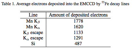
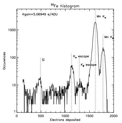
55Fe emits several X-rays at a very specific energy during its decay into 55Mn. X-ray lines of lesser energy are also generated by Auger and other processes within the silicon chip upon exposure to the Kα and Kβ lines. All 55Fe emissions are listed in Table 1 along with the amount of electrons they generate per pixel. Figure 1 shows a typical electron count histogram with respect to the X-ray energy.
One may notice that the source’s photons may scatter its electrons across several adjacent pixels: all images were cleaned from these split events before studying the chip’s CTE.
3.2 Vertical CTE
We evaluated the CCD201-20 vertical charge transfer efficiency using the Mn Kα line average signal with respect to the vertical pixel position. Figure 2 presents the corresponding CTE while controlling the vertical register with a 1 MHz square clock.
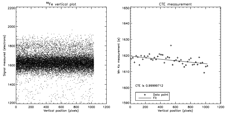
As electrons are created farther from the readout rows, they undergo more transfer losses. Hence the signal decreases with respect to pixel position following a linear trend. The slope of the linear fit directly provides the CTE value for such configuration.
The effects of various clock shapes and frequencies on CTE have been investigated. All data are summarized in Table 2. One key conclusion of these measurements is that vertical charge transfer efficiency is not negatively affected by the use of sinusoidal clocks. In fact, it indicates that CTE is slightly increased when shifting the pixels’ charges with a sinusoidal clock rather than a square clock at the same speed.
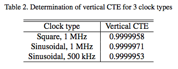
For high-speed applications such as adaptive optics or ultra-fast photometry, it is critical for the clock-induced charges to be at their lowest level for better SNR. It has become apparent that using sinusoidal instead of square clocks enhances an EMCCD’s sensitivity by reducing CIC.6 These results have shown conclusively that the use of sinusoidal clocks reduces the total EMCCD noise resulting in excellent image quality.
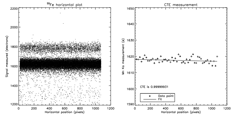
3.3 Horizontal CTE
Before studying the horizontal CTE behaviour through the electron-multiplying register, we performed conventional horizontal charge transfer efficiency measurements following the previous methodology. This time, the clock speed was set at 100 kHz. We obtained a CTE value of 0.9999993, as presented in Figure 3.
However, the regular 55Fe line method does not apply when operating the chip’s EM register. Indeed, when moving through the EM register, all charges undergo the same number of transfer since one want that pixels will exhibit the same gain. To bypass this obstacle, we have used the following method to assess the electron-multiplying register CTE using the same photon source. At first, one must identify all isolated event, then look for the ratio between the second and the main pixels’ signal during transfer. This value provides the fraction of electrons left behind by charge transfer inefficiency in the EM register.
Next, one must infer which part(s) of the horizontal register will affect the charge transfer efficiency. By posing that only the EM register will delay the propagation of charges, the minimal value of the CTE can be given by:

where Pdef is defined as the fraction of delayed electrons. nEM is the number of elements in the EM register (604 for the CCD201-20 chip).
Now assuming that both conventional and EM registries contribute to the CTE, the maximal value of the CTE can be calculated. We thus write
![]()
where nCONV is the number of elements in the conventional horizontal register (1056 for the CCD201-20 chip), while nCONV S represents the number of conventional elements in the extended horizontal register for readout (468 + 16 for the CCD201-20 EMCCD chip). nCONV is divided by 2 as, on average, electrons only travel through half the conventional register.
In the end, the real CTE will fall between CTEmin and CTEmax, depending on the contribution of both types of registers.
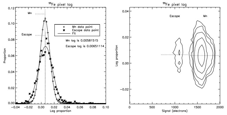
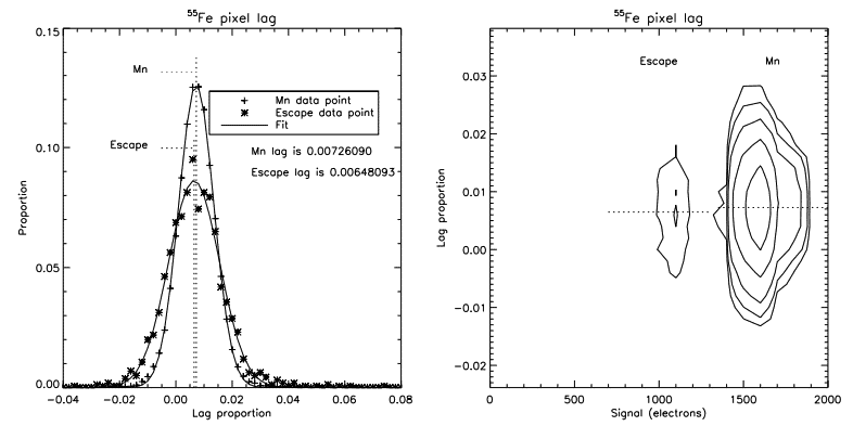
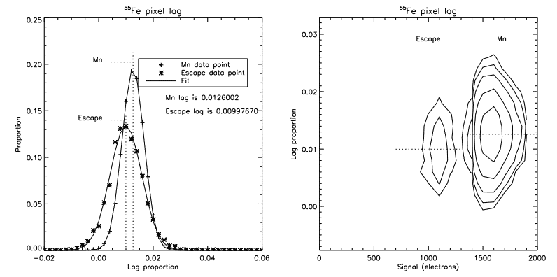
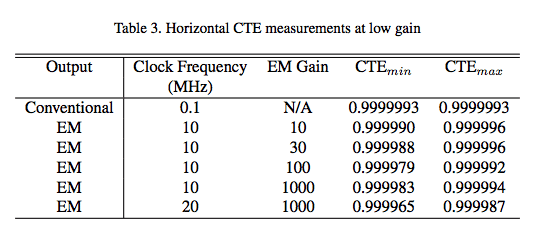
Adopting this methodology, we analyzed the EM register’s CTE at low gains. All data were acquired at 10 MHz. EM gains were set to 10, 30, and 100. Data are plotted in Figures 4 to 6 where the delayed charged fraction distribution is presented for both the Mn and escape α lines. These two lines were used independently to determine the CTE in order to ascertain the validity of the measurement. The lag fraction distribution is also plotted against the source’s signal to show their intensity and spread. Table 3 summarizes the subsequent calculated CTE values.
The growing fraction of delayed charges with increasing gain however suggests that more energetic events occasionally saturate the EM register. Indeed, a signal of about 1700 e¯ passing through the register for a 100 gain yields an average output of 170 ke¯. Still, as the avalanche multiplication is a stochastic process which increases the variance by a factor of 2, the Mn line signal may be strong enough to saturate the EM register from time to time at gains above 100. Moreover, in such conditions, we expect the charge transfer to drop when we get near the saturation level of the multiplication register.
3.4 Horizontal CTE at high EM gain
Because the 55Fe source fails to provide an appropriate signal for high gain data, we sought another method to evaluate the CCD201-20 EM register CTE: by taking dark frames under a high gain, we set the amplified dark current as the signal source. By doing so, it is possible to collect data where pixels containing a dark electron are isolated enough that the probability of having 2 contiguous dark electron is low. Then, by analyzing the ratio of the second pixel to the main, one can infer the minimum and maximum CTE with equations 1 and 2. In this case, the fraction of deferred charge in the second pixel is put against the fraction of “deferred” charges in the pixel before the main pixel. The average value should be null. Measurements were performed at an EM gain of 1000.
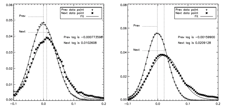
Data were first acquired at 10MHz for comparison with the 55Fe source measurements at the same speed. The left panel of Figure 7 reveals that the amount of deferred charges at a higher EM gain is similar to the one measured with the escape line at an EM gain of 100. The resulting minimum and maximum CTE at an EM gain of 1000 are thus of 0.999983 and 0.999994, respectively. The previous data point being at almost 0 gives confidence in the veracity of the measurement.
The right panel’s data of Figure 7 displays a 2% deferred charges fraction at 20MHz, inferring a minimum and maximum CTE of 0.999965 and 0.999987. It seems that increasing the readout speed reduces charge transfer efficiency. Clocking optimizations are being pursued to raise the CTE at 20MHz.
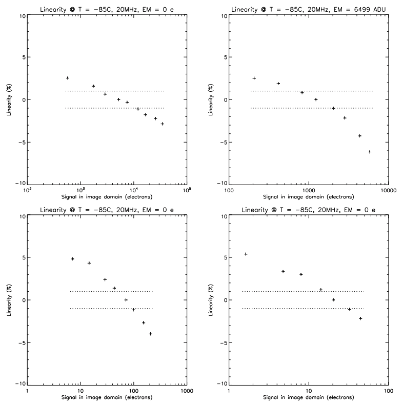
The system’s linearity was measured by exposing the EMCCD to a stabilized light source. As exposure time increases, we expect the measured signal to rise proportionally. In order to yield accurate results, individual image biases were clamped at 300 ADU, thus providing a stable zero-point value set as the dark reference. The EMCCD was operated at −85◦C.
Figure 8 presents the linearity results at 10MHz for various EM gain settings (1, 10, 100, and 1000). When the EM gain was used, the device was operating below its saturation point.
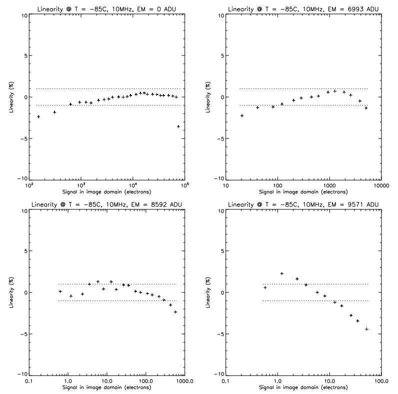
At a unity EM gain, the system’s linearity is very satisfying, remaining within ±1% up to the full well of the CCD201- 20 operated in inverted mode. The linearity measurement at low signal level <500 e¯ is suspected to be affected by the readout noise. At EM gains of 10 and 100, linearity declines slightly, but manages to stay inside the ±1%. Then, at an EM gain of 1000, linearity falls to about 5% at high flux; we believe that the EM gain might be affected by the number of electrons being generated in the multiplication register. As a matter of fact, the electrons effectively decrease the potential well of the high voltage clock, whose amplitude sets the gain’s value. Indeed, at very high gain, a few millivolt amplitude variation of the HV clock may induce gain fluctuations of a few percents.5
We anticipated that the linearity might somewhat suffer when operating the CCD201-20 at 20 MHz as the chip amplifier connected to the EM register settles to 5% at this frequency (in a 20 pF load, as per e2v specifications). Figure 9 shows linearity measurement for the same device operated at a 20 MHz pixel clock. Even though the linearity falls off the ±1% limit, it remains within a reasonable range even at an EM gain of 1000. Throughout our experiment, the linearity behaviour exhibited good stability, and it is expected that one could adjust it with proper characterization.
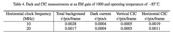
Clock-induced charges assessment requires to collect dark images and overscanning the device into both horizontal and vertical directions. The dark frames integration time was incremented to yield the device’s dark current within the same acquisition. Cosmic rays were cleaned by a sigma clipping algorithm, and affected pixels were replaced by the median of the corresponding pixels of images of same integration time.
The EMCCD imaging area provided the total background signal, which is the outcome of dark current and CIC once cosmic rays are removed. Then, the horizontal overscan region’s signal provided the necessary CIC data generated in both the conventional and EM registers, while the vertical overscan region’s signal was expected to yield the sum of the vertical and horizontal CIC components. A simple subtraction thus lead to the vertical clock-induced charges value.
The exact same vertical clock shape was used for both 10 and 20 MHz pixel frequency. Hence, the vertical CIC, not the dark current was to change between the two acquisitions.
Figure 10 shows the results of the collected CIC data. The data set has also been processed for photon counting by applying a 5σ threshold, then corrected for the proportion of event lost due to the threshold, as determined in [5].
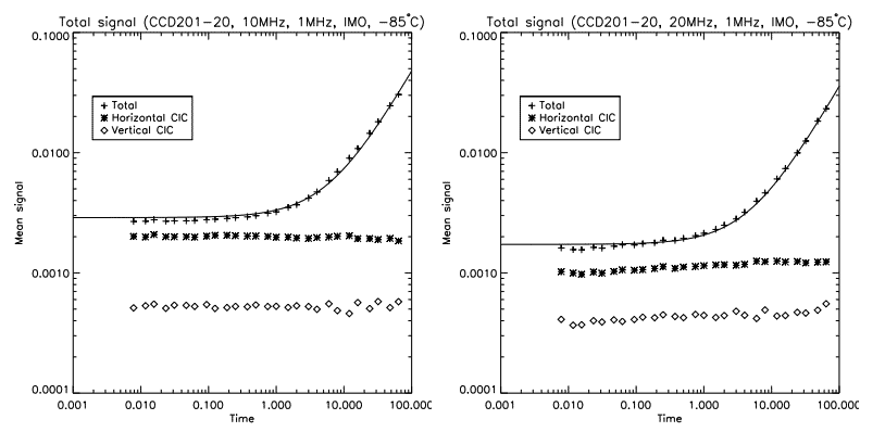
The graphs’ plain lines are linear fits to the data whose slope yields the dark current. The zero-point of the fits leads to the total background signal within a frame. As expected, data show that the vertical CIC and dark current is independent of the horizontal frequency.
Operating the CCD201-20 chip at 20 MHz suggests higher clock speeds reduce the horizontal CIC, by almost a factor of ∼1.5. As a consequence, one could resort to high frame rates and yet obtain the same total background signal.
In this proceeding, we presented our study of a CCD201-20 1k×1k EMCCD from e2v Technologies driven by Nüvü Camēras’ CCCP version 3 controller. The device’s vertical CTE was characterized using both square (conventional) and sinusoidal clocks, which allows for a clock-induced charges decrease even when operating the chip in inverted mode. The EMCCD horizontal register was clocked at 10, and 20 MHz, to determine the behaviour or CTE, linearity and CIC.
Results reveal that the vertical CTE is not negatively impacted while resorting to sinusoidal clocks. In fact, its value is slightly better when the EMCCD was driven by such clocks. This outcome is of importance for photon counting as sinusoidal clocks also lower the total background signal level per frame.
The EM register charge transfer efficiency at 10 MHz and low gain is adequate, although not as high as when it is read at 100 kHz through the conventional amplifier. Even at an EM gain of 1000, the CTE remains high enough so that it does not compromise the photon-counting operating mode. Nevertheless, CTE marginally decreases at 20 MHz. Clocking enhancements are being conducted to counter this effect.
At 10MHz, the EMCCD linearity is excellent and lies under ±1% at a unity EM gain. Still, as the EM gain is increased, the linearity declines slightly. Then, at 20 MHz, the output amplifier settling time worsens the linearity, taking it over ±1%, even at a unity EM gain. As EM gain is raised, linearity follows the same trend than at 10 MHz.
As expected, the vertical clock-induced charges and dark current are not affected by the readout horizontal frequency. However, the horizontal CIC drops as the readout horizontal frequency increases.
Finally, Nüvü Camēras is presently developing a new camera integrating an e2v CCD282 EMCCD 4k×4k chip and CCCPv3 controllers, which will address many high speed applications that require larger fields of view as well as enhanced sensitivity. Differential ultra-fast photometry or high-resolution spectroscopy will greatly benefit from such sensor.
ACKNOWLEDGMENTS
Nüvü Camēras is grateful for the help provided by Prof. Yves Berubé-Lauzière’s team at the Centre Hospitalier Universitaire de Sherbrooke (CHUS): Prof. Roger Lecompte, Dr. Rejean Lebel, Dr. Catherine Pepin, and Mr. Jules Cadorette.
[1] Fontaine, G. and Brassard, P., “The Pulsating White Dwarf Stars,” PASP 120, 1043–1096 (Oct. 2008).
[2] Kreidl, T. J. and Kurtz, D. W., “Frequency analysis of the 5.65-min oscillations in the rapidly oscillating AP star HD 134214,” MNRAS 220, 313–320 (May 1986).
[3] Monet, D. G., Axelrod, T., Blake, T., Claver, C. F., Lupton, R., Pearce, E., Shah, R., and Woods, D., “Rapid Cadence Collections with the Space Surveillance Telescope,” in [American Astronomical Society Meeting Abstracts ], American Astronomical Society Meeting Abstracts 221, 352.17 (Jan. 2013).
[4] Beckers, J. M., “Adaptive optics for astronomy - Principles, performance, and applications,” ARA&A 31, 13–62 (1993).
[5] Daigle, O., Gach, J.-L., Guillaume, C., Lessard, S., Carignan, C., and Blais-Ouellette, S., “CCCP: a CCD controller for counting photons,” in [Society of Photo-Optical Instrumentation Engineers (SPIE) Conference Series ], Society of Photo-Optical Instrumentation Engineers (SPIE) Conference Series 7014 (Aug. 2008).
[6] Daigle, O., Carignan, C., Gach, J., Guillaume, C., Lessard, S., Fortin, C., and Blais-Ouellette, S., “Extreme Faint Flux Imaging with an EMCCD,” PASP 121, 866–884 (Aug. 2009).
[7] Daigle, O., Quirion, P.-O., and Lessard, S., “The darkest EMCCD ever,” in [Society of Photo-Optical Instrumentation Engineers (SPIE) Conference Series ], Society of Photo-Optical Instrumentation Engineers (SPIE) Conference Series 7742 (July 2010).
[8] Janesick, J. R., [Scientific charge-coupled devices ], Scientific charge-coupled devices, Bellingham, WA: SPIE Optical Engineering Press, 2001, xvi, 906 p. SPIE Press monograph, PM 83. ISBN 0819436984 (2001).