We present the progress in characterization of a Nüvü Camēras CCD Controller for Counting Photons (CCCP) designed for extreme low light imaging in space environment with the 1024×1024 Teledyne-e2V EMCCD detector (the CCD201-20). The EMCCD controller was designed using space qualified parts before being extensively tested in thermal vacuum. The performance test results include the readout noise, clock-induced charges, dark current, dynamic range and EM gain. We also discuss the CCCP’s integration in the coronagraph of the High-Contrast Imaging Balloon System project: a fine-pointing and optical payload for a future Canadian stratospheric balloon mission. This first space qualified EMCCD controller, named CCCPs, will enhance sensitivity of the future low-light imaging instruments for space applications such as the detection, characterization and imaging of exoplanets, search and monitoring of asteroids and space debris, UV imaging, and satellite tracking.
Since Electron Multiplying CCD (EMCCD) became commercially available in early 2000, groundbased applications of those devices have flourished: adaptive optics, hyperspectral imaging, high resolution spectroscopy, time-resolved photometry, etc. Although several recent studies were made on the impact of the space environment1–3 on the EMCCD devices for flight applications, very little was published on the optimization of the electronic controller. This paper presents the EMCCD controller developed by Nüvü Camēras for demanding applications of an astronomical space mission, which is based on the same core technology as its commercial EMCCD controllers. This technology has demonstrated its ability to yield low Clock Induced Charges (CIC) as the same time as a low dark current on the CCD60, CCD97, and CCD201-20 from Teledyne-e2v4, 5 and, more recently, on the 4k × 4k CCD282.6 This paper presents the characterization results of the EMCCD space controller in the context of extreme low light imaging for space applications.
The system was designed to clock an EMCCD at a nominal read-out frequency of 10 MHz through its Electron Multiplying (EM) amplifier, as well as to allow the read-out of the EMCCD through its Conventional (CONV) amplifier at low speed and low noise. This allows an EMCCD to operate also as a Charge Coupled Device (CCD), which broadens the incoming light flux range in which the device will reach its maximum efficiency. However, the greatest challenge involved was achieving the same level of CIC with the newly developed system as the one that is achieved with Nüvü Camēras’ commercial cameras. This achievement is required to reach the highest low flux performance.
As the system design inputs we have used the performance goals for the Wide-Field Infrared Survey Telescope (WFIRST) mission from the Table 3.8 of the Science Definition Team (SDT) 2015 document.7 Those criteria and goals are summarized in Tabled 1 and 2, respectively.
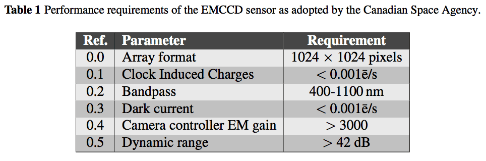
Performance Evaluation Criteria (PEC) 0.2 and performance goals 1.x are met by the use of a CCD201-20 with midband antireflection coating.8 PEC 0.0 and performance goals 2.x are met by the use of a CCD201-20 without the coating.8 The other PEC and performance goals 3.x were dependent on both the EMCCD device used and the controlling electronics. They were checked for compliance.
In order to meet those requirements, the system was designed to provide the following:
• Generation of 14 Low Voltage analog clocks with a refresh rate 160 MHz (6.25 ns) and 14 bits of resolution with a ±15 volts span;
• Generation of 1 High Voltage clock (up to 50 Volts) with a frequency of 10 MHz, a 1 ns timing resolution and an adjustable low and high level with 8 and 12 bits of resolution respectively;
• Digitization of two video outputs (non simultaneously) to accommodate both the EM and Conventional outputs of the CCD201-20. The digitization is be possible at 14 bits, 10 MHz with analog CDS and at 14 bits, 40 MHz with a digital CDS implemented in VHSIC Hardware Description Language (VHDL);
• 10 DC levels with the possibility to adjust them (8 bits);
• A Camera Link (CL) interface for communication of the pixel data to a host and an input for commands.
The goal of the project was to demonstrate that the camera sensitivity was not negatively impacted by the new design of the low and high voltage clocks, the video digitization chains, and the bias generation whilst developing a read-out electronics that was as close as possible to a flight electronics, at a fraction of the cost. Hence, throughout the project, the design aimed to be as close as possible to one that could technically fly even if some aspects of space qualification would not be tested. The system was designed and built with Space Qualified (SQ) or engineering models Integrated Circuits (ICs), or their exact commercial equivalent. The parts were chosen so that the SQ version would sustain the radiation at the environment of L2 orbit for several years. Since the ICs of the controller are either radiation tolerant or radiation hardened by design and it was assembled with a few commercial equivalent parts to save costs, the radiation tolerance was not tested at board-level. The routing of the Printed Circuit Board (PCB) was made with dual footprints to accommodate the SQ and engineering models ICs. Although, the controller did not undergo vibration testing. Best practices usually employed for optimizing the hardware for space applications were employed for the PCB design: the routing was made according to Class 3 of the IPC-2221/2222 standard for the highest level of reproducibility; the board was designed to have a thickness of 93 mils and has several mounting holes to better sustain vibrations; the material of the PCB was chosen to have a low outgassing. The radiation-tolerant Field-programmable Gate Array (FPGA) of the system was not programmed with radiation-aware code. The design phase allocated enough resources required to implement triple redundant logic, watchdogs, etc, but those were not implemented for the tests.
Since the strict requirements of the target mission (WFIRST), such as power, mass, and volume budgets, orbit, launch vehicle, etc have not been finalized, broad assumptions had to be made and several areas of the design could be revisited to better fit a particular mission.
The camera was integrated with a CCD201-20. Two read-out modes were developed to read the EMCCD:
• 10 MHz of horizontal, and 1 MHz of vertical frequencies through the EM amplifier;
• 1 MHz of horizontal, and 1 MHz of vertical frequencies through the CONV amplifier.
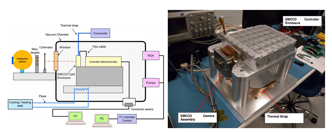
Both of those read-out modes allow for the use of multiple Regions of Interest (ROIs). The tests were performed at ABB’s facilities in Quebec City in a Thermal Vacuum Chamber (TVAC) that was pumped to ∼5·10-7 Torr (Figure 1). The temperature of the electronics was regulated by a Julabo Cooling bath, and the EMCCD was cooled with a Cryomech cryocooler. The temperature of the EMCCD was then read-out with a PT100 Resistance Temperature Detector (RTD) and regulated with a 10 W heater to ±0.01◦C at the sensing point.
The following tests were performed while maintaining the electronics at 20◦C and the EMCCD at -85◦C:
• Characterize the EMCCD and associated controller Read-out Noise (RON) and k-gain at the
fastest pixel rate achievable by the controller;
• Measure the system’s linearity deviation and Vertical Full Well through the EM amplifier;
• Characterize the EMCCD and associated controller RON and k-gain at a slow pixel read-out
through the conventional amplifier;
• Measure the system’s linearity deviation and Vertical Full Well through the CONV amplifier;
Those tests allowed to check the compliance of the system with the PEC 0.5, and performance goals 3.0, 3.4, 3.5, and 3.6.
Next, the temperature of the EMCCD was varied from -75◦C to -105◦C whilst the electronics were kept at 20◦C. The tests performed were the following:
• Characterize the EMCCD gain at the fastest pixel rate achievable by the controller;
• Characterize the CIC generated by the read-out process of the EMCCD gain at the fastest
pixel rate achievable by the controller;
• Characterize the dark current generated by the EMCCD as a function of its temperature.
Those tests allowed to check the compliance of the system with the PEC 0.1, 0.3, 0.4, goals 3.1, 3.2, 3.3, and 3.7.
Then, the temperature of the EMCCD was kept at -85◦C, and the temperature of the electronics were varied from -10◦C to 40◦C. The following tests were the performed:
• Characterize the EMCCD and associated controller RON and k-gain at the fastest pixel rate
achievable by the controller;
• Characterize the EMCCD gain at the fastest pixel rate achievable by the controller.
Finally, the system was exposed to a temperature of 65◦C while unpowered to test for its survival.
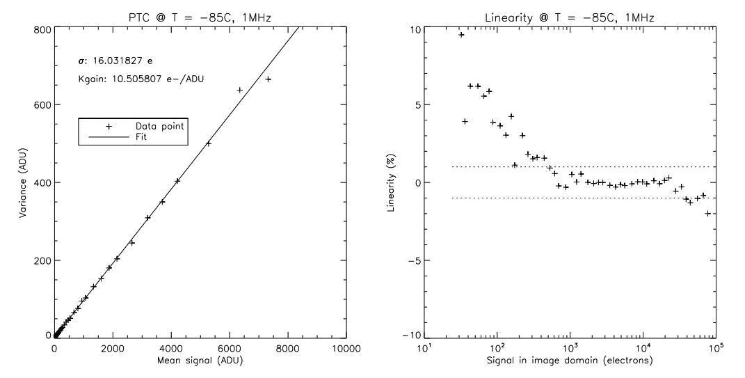
The RON and Vertical Full Well (VFW) are measured by using the Photon Transfer Curve (PTC) method by illuminating EMCCD with a stable light source (LED) while increasing the exposure time to vary the amount of accumulated photons. The method yields at the same time the reciprocal gain of the system (k-gain) and the linearity can be inferred since the the change in the exposure time yields a linearly increasing signal. The RON and k-gain are related to the horizontal shifting and are therefore independent from the VFW if one assumes that the horizontal shifting capacity (e) will always be greater than the vertical shifting capacity. In the case of the CCD201-20, this is true for unity EM gain since the vertical and horizontal charge handling capacity are <80 ke, and >200 ke, respectively. 8
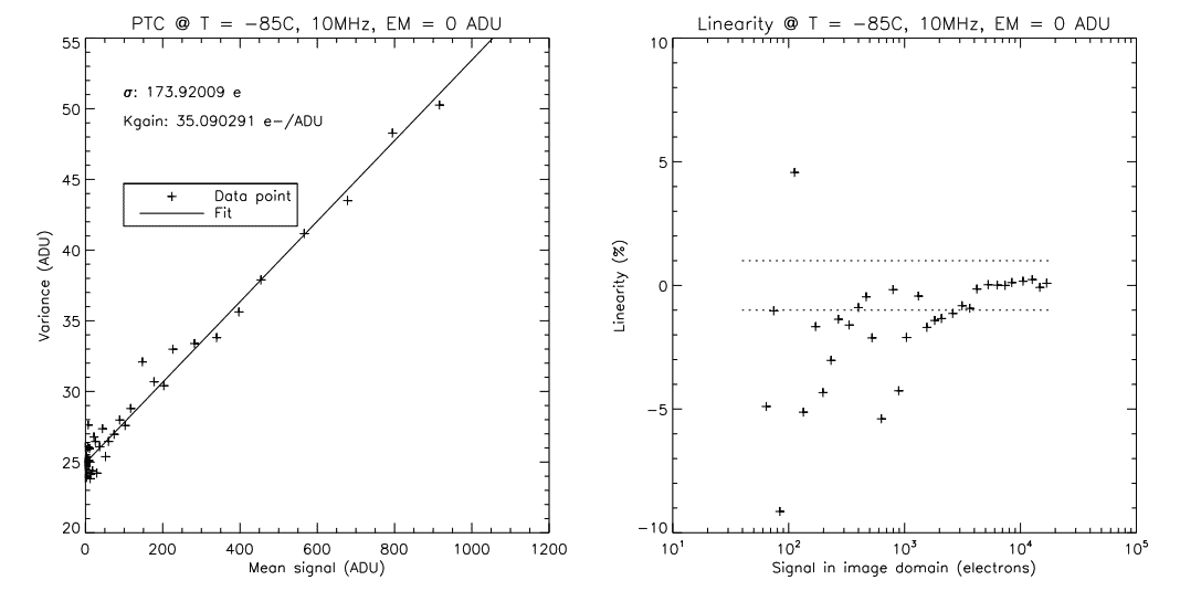
The PTC of the TRL-5 system at 10 MHz through the EM amplifier is shown in Figure 2. The data shows that the system’s response is 35.1 e/ADU, and the read-out noise is 174 e, which means that the standard deviation of a bias image is 4.95 ADU. The acquisition was made with a vertical clocking frequency of 1 MHz, up to a pixel well of ∼35 ke with a linearity within the ±1% range. The linearity at low flux (<10σ) is always a challenge to measure, which explains the scattering of the data points for fluxes <1 ke.
By taking into account the 35 ke of VFW and the RON of 174 e, the dynamic range is of 46 dB with vertical clocks of 1 MHz.
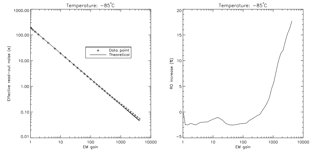
4.2 EM Gain Characterization Through the EM Amplifier at 10 MHz
At temperatures of -75C, -85C, -95C, and -105C, the EM gain and effective RON were measured for logarithmically increasing High Voltage (HV) clock amplitudes. The effective RON as a function of the EM gain was measured through the EM gain characterization process. Since the Excess Noise Factr (ENF) artificially lowers the measured reciprocal gain of the system (k-gain, e/ADU), it has to be taken into account when measuring the effective RON at non-unity EM gain. The measurement of the ENF is made through this process. The theoretical values for the ENF were derived by [9] and are expected to follow the equation

where M is the mean EM gain and N is the number of multiplication elements in the EM register.
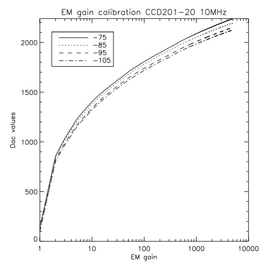
For all temperatures of the EMCCD, the EM gain was calibrated at up to 5000. Figure 3 shows the relation between the command of the HV clock amplitude (controlled by a 12 bits low speed Digital to Analog Converter (DAC)) and the measured EM gain as a function of the temperature of the EMCCD.
The results of effective RON results of shown in Figure 4. The minimum achieved effective RON is <0.05 e. The data shows a slight increase of the effective RON with respect to the theoretical value for EM gains >500. This behaviour is explained by a coupling between the HV clock and the output signal of the EMCCD. A phantom HV clock, that can be explained by substrate bouncing, is observed in the video signal, which creates a correlation between the measured RON and the EM gain. As the HV clock amplitude is increased to yield a higher EM gain, the substrate bouncing becomes higher and so does its effect on the measured RON.
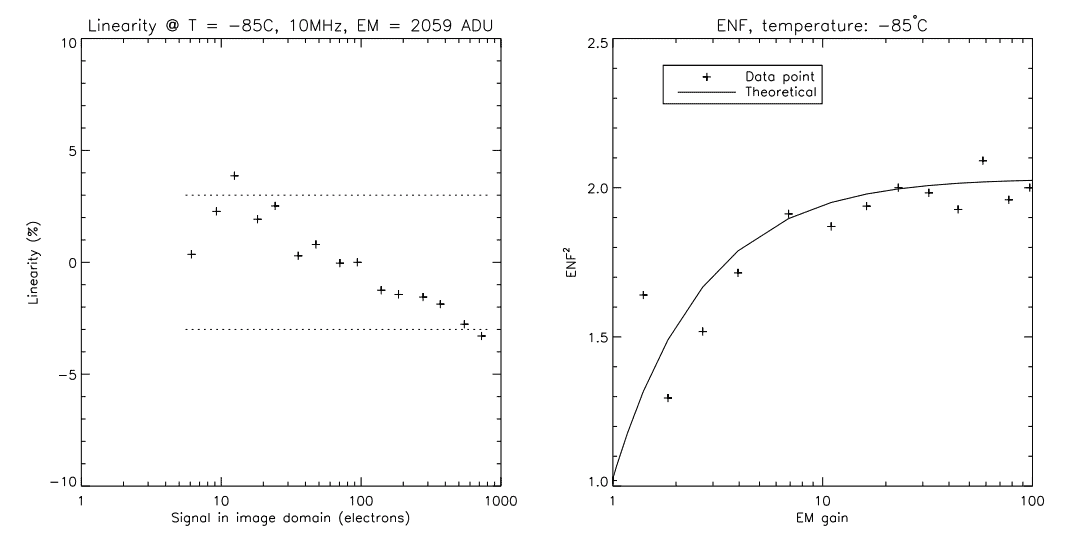
The linearity at an EM gain of 1000 is also measured during the EM gain characterization process. At -85◦C, the EM gain of 1000 is achieved for a DAC value of 2059 Analog to Digital Unit (ADU). Figure 5 shows the linearity measured with the PTC data. The linearity curve is almost fully constrained within the ±3% boundaries up to a full well of ∼400 ke (400 e in the image domain with an EM gain of 1000). This also shows that the EM register Full Well (FW) is >400 ke.
The right panel of Figure 5 shows the measurement of the ENF. Even though the data points are not perfectly aligned with the theoretical curve, the discrepancies should not be associated to an ENF that varies from the predicted value. This simply outlines the fact that the ENF measurement method used does not yield an extremely high Signal to Noise Ratio (SNR). However, the trend of the measured ENF allows one to trust that the EMCCD behaves as predicted by the theory
4.3 Dark Current and CIC Measurements
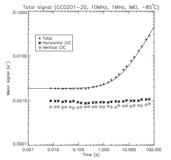
In order to separate the horizontal and vertical CIC components, the EMCCD is over-scanned in both the vertical and horizontal directions (see Figure 6).
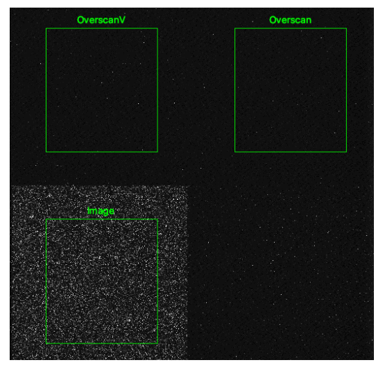
The ”Image” represents the active portion of the detector that is collecting the light. The data for total background signal measurement is taken from this region. The data represents the total unwanted signal that would appear in an image (dark current and CIC). The ”Overscan” is the portion of the detector that undergoes only a horizontal transfer. Hence, the horizontal CIC is measured in this region. Finally, the ”OverscanV” consists of the sum of the horizontal and vertical CIC. Hence, the vertical CIC is taken as the signal level of this region minus the signal of the ”Overscan” region
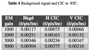
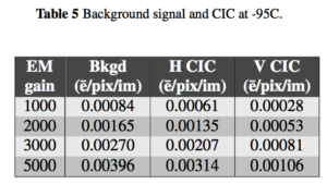
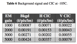
The total background signal was measured with a 0s effective exposure time. Thus, the total background signal measurement includes the dark current generated during the read-out process as well as the CIC. The measurement errors are within 0.0002 e/pixel/im which explains the discrepancy between the total background signal measured and the sum of the horizontal and vertical CIC. The vertical frequency used is 1 MHz, which yields the lowest vertical CIC level. The measurements are made with a 5σ threshold to reflect the Photon Counting operation.
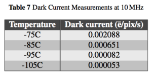
The dark current measurements are performed at an EM gain of 1000. The dark current is measured by fitting a slope to the signal acquired by the camera for exposures from 0 to 64 seconds.
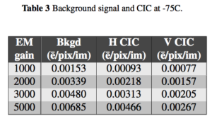
The CIC results are presented in Tables 3 to 6. The dark current results are presented in Table 7. Figure 7 shows an example of the data acquired to measure both the background signal, the horizontal and vertical CIC, as well as the dark current.
The horizontal CIC is roughly independent of the temperature, as it stays around 0.0008 e/pix/im regardless of the temperature, within the measurement errors. The measured vertical CIC does seem to vary with temperature, but it is the impact of the dark current generated during the readout process. Hence, the colder the temperature, the less charges are generated during the read-out. Even though both the horizontal and vertical CIC seem to increase with the EM gain, it is partly the result of the increased photon counting efficiency due to the higher G/σ ratio.10
4.4 RON, Linearity, and VFW Measurements
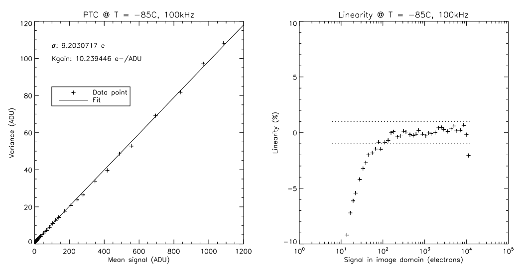
Through the CONV Amplifier at 100 kHz Those measurements were performed with the same method as described in Section 4.1. The Analog to Digital Converter (ADC) of the controller, is not capable of sampling in Correlated Double Sampling (CDS) at 100 kHz (it is limited to 5 MHz). As a result, in order to read-out the EMCCD at 100 kHz of pixel rate, the digital CDS had to be implemented on the controller. This implies to drive the ADC in Sample & Hold (SAH) rather than using its internal CDS, and process the CDS digitally in the FPGA. For that purpose, the ADC is driven at its maximum frequency (40 MHz), which means that a total of 400 samples are acquired for every pixel. The digital CDS is given a table of weights that it applies to the pixel’s samples to properly process the reference, signal, and unwanted samples. Slower read-out would even be possible since the ADC is not the limiting factor. Since the digital CDS can be given up to 2048 weights, it could read-out a CCD or EMCCD as slowly as ∼20 kHz.
An additional benefit of the digital CDS is that it is capable of numerically increasing the signal’s resolution. Even though the ADC is 14 bits, the results of the processing over 400 samples is well beyond the 16 bits resolution. As the theoretical increase in Effective Number of Bits (ENOB) is √(n/4), where n is the number of samples used by the digital CDS, assuming an equal weight for all samples. This feature was not used.
The PTC of the TRL-5 system at 100 kHz through the CONV amplifier is show in Figure 8. The data shows that the system’s response is 10.24e/ADU, and the read-out noise is 9.2 e, which means that the standard deviation of a bias image is 0.9 ADU. The acquisition was made with a vertical clocking frequency of 1 MHz, up to a pixel well of ∼10 ke with a linearity within the ±1% range.
The VFW was also measured with a vertical frequency of 500 kHz, which yields ∼77 ke (Figure 9, with data acquired at 1 MHz pixel rate through the CONV amplifier).
4.5 Temperature Tests
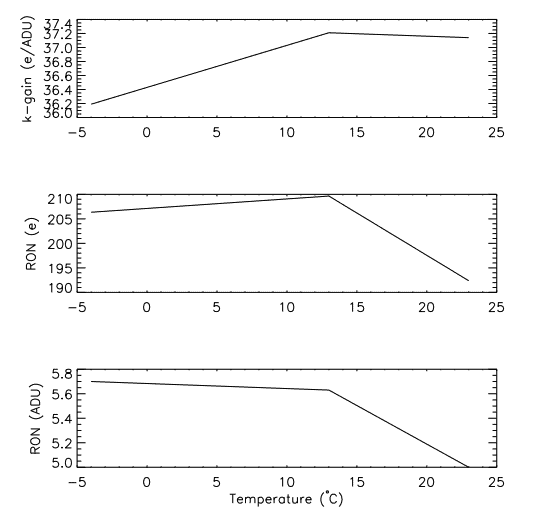
The temperature tests were divided into two parts. The survival test was made in part by baking the controller to 65◦C for 36 hours during the integration to outgas it. Then, it was run at temperatures set points of the cooling bath between -10◦C and 40◦C in 10◦C increments and characterization data at every step. This has the advantage of measuring whether the controller’s response drifts as a function of the temperature.
Hence, a PTC was run at every temperature step increment to measure the response of the EM output when running at 10 MHz. The tests were performed with the core of the controller at -4◦C, 13◦C, and 23◦C. At 33◦C, the controller could not be operated since the FPGA was not perfectly thermally coupled to the housing. Therefore, temperatures warmer than 33◦C were not used. Even though the core of the problem was identified, time constraints prevented to put the controller back in the TVAC for another test run.
The PTC results as a function of the controller’s temperature are presented in Figure 10. The results show a pretty good stability of the k-gain as a function of the temperature. As a matter of fact, they are within 3%, which could be accounted for the measurement errors. The RON (in e) itself does not follow the same trend, and this can be explained by looking at the RON in ADU. There is a tendency of getting a lesser variance in the digital output of the images at the temperature of the controller increases, while the response does not change (k-gain). Hence, the video chains do not seem to exhibit a change in gain, which would affect the k-gain, but they rather exhibit a lesser noise. The exact reason for this behaviour is not yet identified.
The CIC rate measured with the SQ controller was very similar to that achieved with Nüvü Camēras commercial controller. At an EM gain of 1000, the measurements were within the 0.001e/pix/im range for temperatures ≤-85◦C. At warmer temperatures, the CIC measurements were contaminated by the dark current that is generated during the read-out, which is measured in the total background signal.
The minimum dark current achieved at -105◦C was 0.000053 e/pix/s, which is significantly lower than the requirement of 0.001e/pix/s. At -85 ◦C, the dark current measured was 0.000651e/pix/s. It is important to note that the dark current can vary by almost an order of magnitude between devices. Hence, a few devices would have to be tested if a strict specification of dark current would arise for a mission.
The EM gain was characterized up to 5000, which is beyond the 3000 PEC. The controller would be capable of even higher EM gain since its HV clock is capable of a higher amplitude. This gives room for a re-characterization of the EMCCD if an ageing would be measured. In this case, a higher HV clock is required to yield the same EM gain. It is important for the controller to have this capability to ensure that the EMCCD will make it possible to reach very low effective read-out noise through the full extent of a mission.
The dynamic range at 10 MHz and unity EM gain was measured to be 46 dB. A lower RON would benefit the dynamic range. The read-out with a vertical frequency of 500 kHz also improved the dynamic range since the VFW was increased from ∼35 ke to ∼77 ke. The impact of the slower vertical clocks would be to yield a higher level of CIC during the vertical transfer. This was however not measured through this study.
With respect to the WFIRST coronagraph imager’s performance goals, the active area FW and EM register FW were measured and found to meet the goals. The clocking schemes used to fulfill these goals also yield the required CIC level. The linearity of the system was measured to be within the acceptable range, in both EM and CONV modes. The RON of the EM output, at unity EM gain, was found to be higher than the goal. In this case, the 14-bit ADC of the controller, as compared to the 16-bit ADC of Nüvü Camēras’ commercial controller (that led to the 80 e goal), makes it harder to yield a low read-out noise as well as a wide dynamic range (>400 ke in this case). In order to achieve the wide dynamic range while not saturating the ADC, a low response (or high k-gain) has to be implemented. This puts a higher stress on the digitization of the signal since even a low variance of the digitization will yield a high RON. It would be possible to alter the gain of the video chain of the EM output to circumvent this fact and reach a lower RON, at the cost of a lower EM register FW. The same logic applies to the CONV output since it is very difficult to get a RON in ADU that is significantly below 1 ADU. Hence, the high k-gain of the CONV output, required to match the ∼100 ke VFW and allow vertical or horizontal binning, limits the RON one can achieve. In this case, it would be possible to benefit from the increased ENOB made possible by the digital CDS.
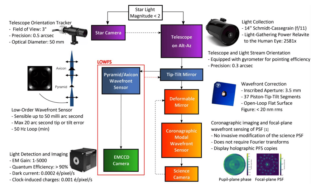
An opportunity arose to fly the SQ system with a 512×512 CCD (CCD97) from Teledyne-e2v in a balloon to image at 40 km of altitude, in the HiCIBaS project11, 12 . The main goal of this mission is to test a Low Order Wavefront Sensor (LOWFS) technology for balloon-based exoplanet imaging to compensate for inadequate pointing accuracy as well as to gather data about the atmospheric dynamics that are prevalent at the balloon altitude, which are mandatory for precision astronomy. This application has been identified as a pathfinder to future potential mission employing high contrast imaging. The schematic diagram of the HiCiBaS payload is presented in Figure 11. This concept outlines a complete system that would be required to image exoplanets with the help of a coronagraph.
While the primary objective of the project remains the study and characterization of the LOWFS performance at 40 km and the typical PSF instabilities and anomalies encountered at these altitudes in the visible, this testbed allows further expansion into a more complete high contrast imaging observatory to be flown for dedicated exoplanet candidate observations. Follow-on activities that were suggested in the original project included:
1. Addition of a coronagraph and high sensitivity EMCCD camera.
2. Addition of a Deformable Mirror to further refine star flux rejection and WFEs control.
3. Replacement of the telescope for a larger unobscured aperture system (ex. 70 cm TMA similar to PILOT).
4. Addition of an Integral Field Spectrograph to perform spectroscopic observation of exoplanet candidates.
In the full mission concept, there are two cameras. The first one is a fast camera that is embedded in the LOWFS block (see also Figure 12), which in this case is a HNu 128 that N ¨ uv¨ u Cam ¨ eras ¯ provides to the project. The second camera is the ”science camera” that would be used to image the output of the coronagraph.
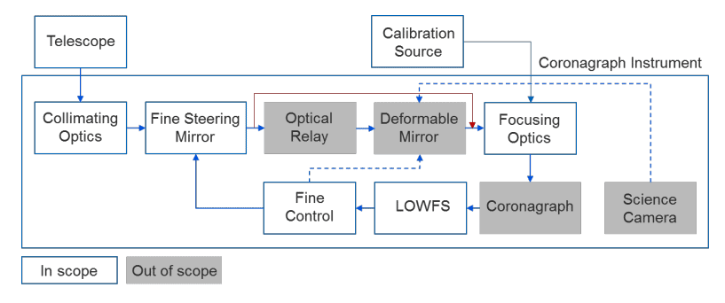
6.1 The coronagraph arm
The original HiCIBaS mission involves testing only the LOWFS. Hence, the coronagraph parts are out of scope. However, the evolution of this mission has raised interests among the scientific community to fly not only the LOWFS, but the coronagraph system as well. The following contributions have become available from collaborators: the Deformable Mirror (DM) is provided by Iris-AO, the coronagraph13 is provided by the Leiden University (Netherlands), the Real-Time Computer (RTC) is provided by the NASA, and Nüvü Camēras proposed to provide the science camera using the SQ controller that was developed.
Subsequently, the optical design of the HiCiBaS mission was thus modified to include the coronagraph arm (Figure 13) with the added components. On this figure, the ”EMCCD 128” camera is the camera for the LOWFS, while the ”EMCCD 512” camera is the science camera for the coronagraph arm. An example of the image at the focal plane of the science camera is shown in Figure 14. The crowding of the spatial structures that has to be imaged explains the relatively high spatial resolution that is required for this mission. Moreover, the space constraints on the balloon platform limits the length of the coronagraph bench to